
could Nintendo been hiring a hardware tester for it next console?(problaby not)
Could be for BC?
could Nintendo been hiring a hardware tester for it next console?(problaby not)
I would assume similar to most photomasks that they use e-beam lithography. Which, yeah is very slow but very precise to the single digit nm level.Canon apparently use lasers to precisely heat both the mask and the wafer itself. As they have different thermal expansion coefficients, they can use the heating to move the mask relative to the wafer.
I'm curious how they make the actual masks/moulds themselves. I suppose it's not quite as relevant, given a mask will be used a very large number of times, so the manufacturing process for masks can be slow and expensive, but as the starting point for "how to make things with very tiny features" starts with "take your mask that already has very tiny features on it...", it's an inevitable point of curiosity. Particularly so as, unlike photolithography, there's no optical reduction, so the mask needs to be at the exact final feature size, not several times larger. Of course they don't have to worry about calculating the interference patterns required to produce the desired features, so that removes one tricky step from the process.
I don't think we have had nvidia-esque leaks in the past till now, which makes things pretty different IMHO.In history has there ever been rumors on specs for a Nintendo console where everyone believed to be true and it actually ended up being the case on final specs?
could Nintendo been hiring a hardware tester for it next console?(problaby not)
That’s one way to look at it. This is going to be very interesting.I don't think we have had nvidia-esque leaks in the past till now, which makes things pretty different IMHO.
could Nintendo been hiring a hardware tester for it next console?(problaby not)
could Nintendo been hiring a hardware tester for it next console?(problaby not)
I'm not sure what the other ways to look at this is, but yes, it's going to be interesting to see if anything has changed from the findings based on March 2022 nvidia leak and the present (or rather, when we first find out the full specifications of Switch 2).That’s one way to look at it. This is going to be very interesting.
If adapter pedestal isn't a dock, I'd be very surprised.I'm not sure what the other ways to look at this is, but yes, it's going to be interesting to see if anything has changed from the findings based on March 2022 nvidia leak and the present (or rather, when we first find out the full specifications of Switch 2).
There are shipment records of items (functional test PCAs, Carpa dev kits, and an "adaptor pedestal" which is probably a boring accessory) associated to T239 all the way up to May 2023 as the latest occurrence. Have almost no reason to believe it's anything other than T239.
I don't think you can call games that sell 20+ million units in a few weeks a "minority". In quantity? Yes, but a single AAA game makes as much revenue as a hundred indie and similar games, the money they generate far outweighs the quantity of them (which is totally fine given raising costs and turnaround times).Big budget AAA or even AA games are in a minority. Switch could be getting 0 of them and it would still be possible to be getting most of the same third party content. At least by the numbers, though one Assassin's Creed might have taken the budget and human hours of a few hundred indie releases.
The adaptor pedestal was something for chip testing.I'm not sure what the other ways to look at this is, but yes, it's going to be interesting to see if anything has changed from the findings based on March 2022 nvidia leak and the present (or rather, when we first find out the full specifications of Switch 2).
There are shipment records of items (functional test PCAs, Carpa dev kits, and an "adaptor pedestal" which is probably a boring accessory) associated to T239 all the way up to May 2023 as the latest occurrence. Have almost no reason to believe it's anything other than T239.
Not unless they've shrunk the dock to 22 square millimeters!If adapter pedestal isn't a dock, I'd be very surprised.
Wouldn't that be about what we'd expect the SOC of the dock to be sized at, though?The adaptor pedestal was something for chip testing.
But yes, there is no remotely plausible argument for the chip not being T239. There really hasn't been since March 2022, and the shipping listings aren't even the only reconfirmation since then, but they are the most recent and are public and should be understandable to everyone.
Not unless they've shrunk the dock to 22 square millimeters!
could Nintendo been hiring a hardware tester for it next console?(problaby not)
The company that shipped it is a developer of tools for electrical characterization/validation, and adaptor pedestal sounds enough like something you would use to do that, so that's probably what it is. We can't draw any specifics about it based on the size or the description, but there's nothing that indicates it's related to the dock or a console accessory.Wouldn't that be about what we'd expect the SOC of the dock to be sized at, though?
That said- it could be a VERY LITERAL adapter pedestal. You plop a chip on the pedastal and it adapts its pins out to something human hands can manipulate.
With that said- that would be an extraordinary small pedestal in that case, so maybe it helps us consider the size of the T239 chip itself - a 22mm^2 platform would easily fit it with room for connectors if it was made on 4N.
The company in question is massive and employs 11k people -- hell, they own random studios like High-Voltage. The job listing could be related to anything.Eh, yeah who knows. But the fact that 9 Nintendo "alumni" work there is a stretch (and again this is also a LinkedIn choose-your-own-adventure thing). How many "alumni" from Microsoft work there? It doesn't pop up cause he's not searching for that. But I'd bet all my famicoins it ain't zero.
Job listing on the company's site also says "Ongoing Contract, Expected through June 2024 with possibility of extension". No idea what it's for, but probably could have added that detail, for whatever that's worth. https://apply.workable.com/keywords-intl1/j/63138CE62B/
We can pretty safely assume it's less than 22 square millimeters, that's a start.The company that shipped it is a developer of tools for electrical characterization/validation, and adaptor pedestal sounds enough like something you would use to do that, so that's probably what it is. We can't draw any specifics about it based on the size or the description, but there's nothing that indicates it's related to the dock or a console accessory.
MS is releasing essentially just a die shrink, probably won't require a ton of testing.Eh, yeah who knows. But the fact that 9 Nintendo "alumni" work there is a stretch (and again this is also a LinkedIn choose-your-own-adventure thing). How many "alumni" from Microsoft work there? It doesn't pop up cause he's not searching for that. But I'd bet all my famicoins it ain't zero.
Job listing on the company's site also says "Ongoing Contract, Expected through June 2024 with possibility of extension". No idea what it's for, but probably could have added that detail, for whatever that's worth. https://apply.workable.com/keywords-intl1/j/63138CE62B/
That @Thraktor post needs an update.
thanks for this, I have been lurking on here for a long time and really am here for the hardware speculationI was away when this was posted, so didn't get a chance to reply, but as there were a few more references over the past couple of pages, I thought I'd come back to it.
Firstly, my post wasn't intended to be a guide to what clock speeds people should expect for Switch 2. The intent of the post was to explain that there's a lower bound to clock speeds in portable mode; that you can't just clock down to oblivion on an inefficient process, and that the evidence suggests that the T239's GPU on 8nm at this lower bound would still consume far too much power for a device like the Switch. Therefore, I think it's more likely that the manufacturing process is TSMC 4N.
The clock speed estimates were just something I included in the post as a guess, because other people were guessing clock speeds before that and I joined in. I'm just a random person on the internet with no inside knowledge or expertise in the area, and my guesses aren't any more likely to be right or wrong than anyone else's. They should be taken with a reasonable margin of error.
That said, I don't think my estimates need to be updated. In fact, I don't think differences in manufacturing process or the size of the Switch 2 really make much difference to my performance expectations at this stage.
To explain, there are two different practical limits on the GPU performance of the Switch 2. In portable mode, there is the lower bound on clocks, as discussed above. Then, in docked mode, there is an effective upper bound on GPU clocks, the point where the GPU becomes completely bandwidth-limited, based on the total bandwidth that a 128-bit LPDDR5 bus can provide. We don't know the exact points of either of these things, but let's say for the sake of argument, that 500MHz is the lower bound on portable clock speeds. Bandwidth limitations are a bit more complex, as some games may be more or less bandwidth-limited than others, but again just for the sake of argument let's say 1.2GHz is the limit for clocks in docked mode; above this the GPU is bandwidth-limited.
From Nintendo's point of view, there's another limit on GPU performance; they want the relative performance between docked and portable mode to be relatively consistent with the difference in rendering resolutions across both modes. The difference in output resolutions will be much higher than it was on the Switch (a 4x difference between 1080p portable and 4K docked), but with DLSS scaling the standard, Nintendo will likely expect internal rendering resolutions to be closer to a 2x ratio for practicality's sake. If the difference in performance between the modes goes too far askew it will become increasingly difficult for developers to make games which properly leverage both modes and look good and perform well on both modes.
So let's say, hypothetically, T239 is manufactured on TSMC's 4N process, is even more efficient than we expected, and Nintendo have also decided to make the Switch 2 an enormous Steam Deck-sized beast with a giant battery so that they can sustain lots of power draw in portable mode. Let's say that in doing so, they could push the portable GPU clock all the way up to 800MHz. Would they actually want to do that? Probably not, at my guess.
At 800MHz portable, and with a (hypothetical) cap of 1.2GHz docked, Nintendo's developers would be in an awkward position, as they have to output 4x as many pixels in docked mode, but only have 50% more power to do so. One option would be to add a lot of graphical effects to the portable mode and disable them from the docked mode, but this just adds extra work for the development team, and they would be adding graphical effects to the mode where they're less noticeable.
Another option would be to just run at, or very close to, native resolution in portable mode, and rely more heavily on DLSS in docked mode. But if you choose, let's say 900p scaled via DLSS to 1080p in portable mode, and 1080p scaled up to 4K (or even just 1440p) in docked, you're kind of wasting that portable mode power. A 720p internal rendering resolution scaled to 1080p via DLSS would be almost indistinguishable from 900p internal to most people (particularly on a small screen), so you may as well just clock back down to 500-600MHz anyway and render at around 720p. And hey, now you get much better battery life and/or don't need to make Switch 2 a Steam Deck-sized giant anymore, so it's a win all round.
Of course these are entirely hypothetical numbers, and none of us know the precise minimum clock in portable mode, or the point where bandwidth becomes the major constraint in docked mode, but even with rough guesses, there isn't much room to manoeuvre. Based on what we know, and assuming Nintendo want to keep around a 2x ratio between portable and docked clocks, then regardless of manufacturing process I'd be expecting a range of 500-600MHz portable and 1.0-1.2GHz docked. You can go much higher or much lower than these without getting into very inefficient clocks in portable or becoming heavily bandwidth constrained docked. Hence my guess, which is right in the middle of those ranges.
Strictly speaking, we don't have 100% confirmation that it's using LPDDR5 yet, and it could in theory be using LPDDR5X which would allow it to hit higher clocks in docked mode before becoming bandwidth constrained, but I'm assuming LPDDR5 until we get very good evidence otherwise. Even on 4N I could see cooling becoming the bottleneck in docked mode before LPDDR5X becomes necessary.
It's subjective. Not a fact.Switch is a 9th Generation hybrid platform. That is a fact
IF Nintendo want's the gimmick of this next console to be SUPER POWER (on the go!) then they may actually be going with something more cutting edge like LPDDR5X. And IF that is the case they can then push the docked clocks all the way past the point (somewhere around 1.5 to 1.6GHz) of achieving a 4TF machine. If they plan to market the power of it that would take them to the point where they could literally say more powerful than an Xbox (Series S very small at the bottom in the legal copy).I was away when this was posted, so didn't get a chance to reply, but as there were a few more references over the past couple of pages, I thought I'd come back to it.
Firstly, my post wasn't intended to be a guide to what clock speeds people should expect for Switch 2. The intent of the post was to explain that there's a lower bound to clock speeds in portable mode; that you can't just clock down to oblivion on an inefficient process, and that the evidence suggests that the T239's GPU on 8nm at this lower bound would still consume far too much power for a device like the Switch. Therefore, I think it's more likely that the manufacturing process is TSMC 4N.
The clock speed estimates were just something I included in the post as a guess, because other people were guessing clock speeds before that and I joined in. I'm just a random person on the internet with no inside knowledge or expertise in the area, and my guesses aren't any more likely to be right or wrong than anyone else's. They should be taken with a reasonable margin of error.
That said, I don't think my estimates need to be updated. In fact, I don't think differences in manufacturing process or the size of the Switch 2 really make much difference to my performance expectations at this stage.
To explain, there are two different practical limits on the GPU performance of the Switch 2. In portable mode, there is the lower bound on clocks, as discussed above. Then, in docked mode, there is an effective upper bound on GPU clocks, the point where the GPU becomes completely bandwidth-limited, based on the total bandwidth that a 128-bit LPDDR5 bus can provide. We don't know the exact points of either of these things, but let's say for the sake of argument, that 500MHz is the lower bound on portable clock speeds. Bandwidth limitations are a bit more complex, as some games may be more or less bandwidth-limited than others, but again just for the sake of argument let's say 1.2GHz is the limit for clocks in docked mode; above this the GPU is bandwidth-limited.
From Nintendo's point of view, there's another limit on GPU performance; they want the relative performance between docked and portable mode to be relatively consistent with the difference in rendering resolutions across both modes. The difference in output resolutions will be much higher than it was on the Switch (a 4x difference between 1080p portable and 4K docked), but with DLSS scaling the standard, Nintendo will likely expect internal rendering resolutions to be closer to a 2x ratio for practicality's sake. If the difference in performance between the modes goes too far askew it will become increasingly difficult for developers to make games which properly leverage both modes and look good and perform well on both modes.
So let's say, hypothetically, T239 is manufactured on TSMC's 4N process, is even more efficient than we expected, and Nintendo have also decided to make the Switch 2 an enormous Steam Deck-sized beast with a giant battery so that they can sustain lots of power draw in portable mode. Let's say that in doing so, they could push the portable GPU clock all the way up to 800MHz. Would they actually want to do that? Probably not, at my guess.
At 800MHz portable, and with a (hypothetical) cap of 1.2GHz docked, Nintendo's developers would be in an awkward position, as they have to output 4x as many pixels in docked mode, but only have 50% more power to do so. One option would be to add a lot of graphical effects to the portable mode and disable them from the docked mode, but this just adds extra work for the development team, and they would be adding graphical effects to the mode where they're less noticeable.
Another option would be to just run at, or very close to, native resolution in portable mode, and rely more heavily on DLSS in docked mode. But if you choose, let's say 900p scaled via DLSS to 1080p in portable mode, and 1080p scaled up to 4K (or even just 1440p) in docked, you're kind of wasting that portable mode power. A 720p internal rendering resolution scaled to 1080p via DLSS would be almost indistinguishable from 900p internal to most people (particularly on a small screen), so you may as well just clock back down to 500-600MHz anyway and render at around 720p. And hey, now you get much better battery life and/or don't need to make Switch 2 a Steam Deck-sized giant anymore, so it's a win all round.
Of course these are entirely hypothetical numbers, and none of us know the precise minimum clock in portable mode, or the point where bandwidth becomes the major constraint in docked mode, but even with rough guesses, there isn't much room to manoeuvre. Based on what we know, and assuming Nintendo want to keep around a 2x ratio between portable and docked clocks, then regardless of manufacturing process I'd be expecting a range of 500-600MHz portable and 1.0-1.2GHz docked. You can go much higher or much lower than these without getting into very inefficient clocks in portable or becoming heavily bandwidth constrained docked. Hence my guess, which is right in the middle of those ranges.
Strictly speaking, we don't have 100% confirmation that it's using LPDDR5 yet, and it could in theory be using LPDDR5X which would allow it to hit higher clocks in docked mode before becoming bandwidth constrained, but I'm assuming LPDDR5 until we get very good evidence otherwise. Even on 4N I could see cooling becoming the bottleneck in docked mode before LPDDR5X becomes necessary.
I doubt they'll be blatant- and I'll doubt they'll sacrifice thickness to achieve it, but I DO expect Nintendo to advertise POWER this generation. They did it a little with Switch around launch, but now that POWER is the primary differentiator between it and Switch, it'll be more worthwhile to indulge.IF Nintendo want's the gimmick of this next console to be SUPER POWER (on the go!) then they may actually be going with something more cutting edge like LPDDR5X. And IF that is the case they can then push the docked clocks all the way past the point (somewhere around 1.5 to 1.6GHz) of achieving a 4TF machine. If they plan to market the power of it that would take them to the point where they could literally say more powerful than an Xbox (Series S very small at the bottom in the legal copy).
NOW YOUR PLAYING WITH POWER. SUPER POWER.
Super Nintendo Switch.
March 22.
But probably not.
Sorry it's taken me so long to write a reply - work has kept me very busy lately. I know that you understand neural networks, Thraktor, but I've still structured this as a longer explanation post so that people with less experience than you can also engage with my argument. The reason my thinking on this has shifted a bit is that removing layers in a convolutional autoencoder for performance reasons isn't a simple change.You're correct in that any attempt to reduce the performance cost of DLSS would impact image quality, but I don't think that's necessarily always a bad thing. When developing DLSS, Nvidia would have had to find a balance between image quality and speed. You can always use a bigger, more complex network (so long as you have sufficient training data) to get better quality*, or a smaller, simpler network to get better performance, and we can assume that DLSS currently represents what Nvidia believes to be the sweet spot, where moving in either direction wouldn't be a worthwhile trade-off.
However, the sweet spot between speed and quality for desktop GPUs isn't necessarily the same as the sweet spot for portable devices with a fraction of the performance. Different trade-offs apply, and what might be considered cheap on a desktop GPU might take an unreasonable portion of the frame time on a low-power console. Even the quality trade-offs may differ, as IQ issues that may be noticeable to someone sitting right in front of a computer monitor may not be as noticeable on a TV screen further away, or a much smaller handheld screen.
I'm sure Nvidia is and will continue to provide the standard versions of DLSS to Switch developers to use in their games, and I don't think there's any free lunch where Nintendo gets a DLSS implementation that's magically faster without any trade-offs, but I do think that there's potentially value, in addition to regular DLSS, to providing a more light-weight version of the model as an option for developers who are comfortable sacrificing a bit of image quality for performance. Whether that's because they're stretching to squeeze in their chosen lighting model and feel it's important enough to sacrifice a bit of IQ by cutting down DLSS time, or because they're targeting 60fps and prefer using DLSS-lite to hit 4K rather than the 1440p output of regular DLSS, or because the limitations of DLSS-lite simply aren't readily apparent in their game (say it has more artifacting around certain high-frequency detail patterns, but they're not present).
* To a certain point. I assume that you'll asymptotically approach "ideal" IQ for the amount of input data you have, and adding excess complexity for this particular task may end up over-fitting or hallucinating, which wouldn't be desirable.


Yes Nintendo does produce some of the best, but C'mon about the last part.Nintendo already produces some of the best graphics in the entire industry, full stop. Personally, I haven’t seen a PS5/XS title that impresses me more.
Ok. Nevermind.Astro and Sackboy have games which are no better than the Wii U’s Super Mario 3D World
actuallly all they'd need to FLOP-Match the Series S is ~1.3GHz with the 12SM config in Switch 2.IF Nintendo want's the gimmick of this next console to be SUPER POWER (on the go!) then they may actually be going with something more cutting edge like LPDDR5X. And IF that is the case they can then push the docked clocks all the way past the point (somewhere around 1.5 to 1.6GHz) of achieving a 4TF machine. If they plan to market the power of it that would take them to the point where they could literally say more powerful than an Xbox (Series S very small at the bottom in the legal copy).
NOW YOUR PLAYING WITH POWER. SUPER POWER.
Super Nintendo Switch.
March 22.
But probably not.
So what does a 1.6GHz clock get you?actuallly all they'd need to FLOP-Match the Series S is ~1.3GHz with the 12SM config in Switch 2.
The 1.38GHz in the DLSS Tool thing is a bit overkill for that specific metric reporting back 4.23TFLOPs
A trillion flip flops.So what does a 1.6GHz clock get you?
no one knowsSo what does a 1.6GHz clock get you?
A Big Mac with medium fries? IdkSo what does a 1.6GHz clock get you?
Why notI've been meaning to ask, why???

shit man that's why I've been defending it in the other threadWhy not
I mean if you believe Nate that's exactly what happened when Nintendo supposedly recalled their dev kits..
You would have to delay game development or have third parties sit on their games. It would mean they would have to delay production,
I mean if Kopite it's right about 8nm, it wont the much more dated in 2025 than 2024zheck might run into the problem that their node or tech starts to be outdated.
MY HAT HAS BEEN THROWN INTO THE RING
this recall of devkit Nate has stated, is for the hipotetical Switch Pro, not Switch sucessorI mean if you believe Nate that's exactly what happened when Nintendo supposedly recalled their dev kits.
To be clear, I don't believe that.
I mean if Kopite it's right about 8nm, it wont the much more dated in 2025 than 2024z
There are other threads??shit man that's why I've been defending it in the other thread
carry on
this recall of devkit Nate has stated, is for the hipotetical Switch Pro, not Switch sucessor
That could be an argument for 2025.That's bullshit. You don't plan to release a pro, cancel it and release a successor a year later.
At most they rebranded Drake from a pro to a successor, but I doubt that too.
This bigger sticking point with bigger differences between Docked and Portable are really cooling and too big a divide between Portable and Docked. As Thraktor said, having too big a difference between each mode would basically make developers create double SKU/double the work but only reap the reward once. An uninteresting proposition.You could then introduce a much bigger and quieter active cooling solution via the dock itself which would simply push the air through the device in docked mode allowing for a much higher thermal limit which if we have more bandwidth perhaps could be on the table
I was away when this was posted, so didn't get a chance to reply, but as there were a few more references over the past couple of pages, I thought I'd come back to it.
Firstly, my post wasn't intended to be a guide to what clock speeds people should expect for Switch 2. The intent of the post was to explain that there's a lower bound to clock speeds in portable mode; that you can't just clock down to oblivion on an inefficient process, and that the evidence suggests that the T239's GPU on 8nm at this lower bound would still consume far too much power for a device like the Switch. Therefore, I think it's more likely that the manufacturing process is TSMC 4N.
The clock speed estimates were just something I included in the post as a guess, because other people were guessing clock speeds before that and I joined in. I'm just a random person on the internet with no inside knowledge or expertise in the area, and my guesses aren't any more likely to be right or wrong than anyone else's. They should be taken with a reasonable margin of error.
That said, I don't think my estimates need to be updated. In fact, I don't think differences in manufacturing process or the size of the Switch 2 really make much difference to my performance expectations at this stage.
To explain, there are two different practical limits on the GPU performance of the Switch 2. In portable mode, there is the lower bound on clocks, as discussed above. Then, in docked mode, there is an effective upper bound on GPU clocks, the point where the GPU becomes completely bandwidth-limited, based on the total bandwidth that a 128-bit LPDDR5 bus can provide. We don't know the exact points of either of these things, but let's say for the sake of argument, that 500MHz is the lower bound on portable clock speeds. Bandwidth limitations are a bit more complex, as some games may be more or less bandwidth-limited than others, but again just for the sake of argument let's say 1.2GHz is the limit for clocks in docked mode; above this the GPU is bandwidth-limited.
From Nintendo's point of view, there's another limit on GPU performance; they want the relative performance between docked and portable mode to be relatively consistent with the difference in rendering resolutions across both modes. The difference in output resolutions will be much higher than it was on the Switch (a 4x difference between 1080p portable and 4K docked), but with DLSS scaling the standard, Nintendo will likely expect internal rendering resolutions to be closer to a 2x ratio for practicality's sake. If the difference in performance between the modes goes too far askew it will become increasingly difficult for developers to make games which properly leverage both modes and look good and perform well on both modes.
So let's say, hypothetically, T239 is manufactured on TSMC's 4N process, is even more efficient than we expected, and Nintendo have also decided to make the Switch 2 an enormous Steam Deck-sized beast with a giant battery so that they can sustain lots of power draw in portable mode. Let's say that in doing so, they could push the portable GPU clock all the way up to 800MHz. Would they actually want to do that? Probably not, at my guess.
At 800MHz portable, and with a (hypothetical) cap of 1.2GHz docked, Nintendo's developers would be in an awkward position, as they have to output 4x as many pixels in docked mode, but only have 50% more power to do so. One option would be to add a lot of graphical effects to the portable mode and disable them from the docked mode, but this just adds extra work for the development team, and they would be adding graphical effects to the mode where they're less noticeable.
Another option would be to just run at, or very close to, native resolution in portable mode, and rely more heavily on DLSS in docked mode. But if you choose, let's say 900p scaled via DLSS to 1080p in portable mode, and 1080p scaled up to 4K (or even just 1440p) in docked, you're kind of wasting that portable mode power. A 720p internal rendering resolution scaled to 1080p via DLSS would be almost indistinguishable from 900p internal to most people (particularly on a small screen), so you may as well just clock back down to 500-600MHz anyway and render at around 720p. And hey, now you get much better battery life and/or don't need to make Switch 2 a Steam Deck-sized giant anymore, so it's a win all round.
Of course these are entirely hypothetical numbers, and none of us know the precise minimum clock in portable mode, or the point where bandwidth becomes the major constraint in docked mode, but even with rough guesses, there isn't much room to manoeuvre. Based on what we know, and assuming Nintendo want to keep around a 2x ratio between portable and docked clocks, then regardless of manufacturing process I'd be expecting a range of 500-600MHz portable and 1.0-1.2GHz docked. You can go much higher or much lower than these without getting into very inefficient clocks in portable or becoming heavily bandwidth constrained docked. Hence my guess, which is right in the middle of those ranges.
Strictly speaking, we don't have 100% confirmation that it's using LPDDR5 yet, and it could in theory be using LPDDR5X which would allow it to hit higher clocks in docked mode before becoming bandwidth constrained, but I'm assuming LPDDR5 until we get very good evidence otherwise. Even on 4N I could see cooling becoming the bottleneck in docked mode before LPDDR5X becomes necessary.
Sorry it's taken me so long to write a reply - work has kept me very busy lately. I know that you understand neural networks, Thraktor, but I've still structured this as a longer explanation post so that people with less experience than you can also engage with my argument. The reason my thinking on this has shifted a bit is that removing layers in a convolutional autoencoder for performance reasons isn't a simple change.
Three features of a convolutional autoencoder
Working principle of all autoencoders: make the network choose which features matter
An autoencoder is essentially two neural networks concatenated with each other: the encoder, which chooses which features are important, and the decoder, which does reconstruction. By design, the encoder gives up information about the input in each layer; the idea is to force the network to make decisions about which information is relevant to reconstruction.
The more mathematical way to say this is that the encoder learns a representation of the input in a lower dimensional latent space, then the decoder uses the latent space representation to reconstruct the output in a higher dimensional space. This means that, in the encoder, the dimension of each layer needs to be strictly less than or equal to the previous layer; in the decoder, the opposite is true. Another way to think about it is that the encoder is finding an ideal compressed representation of the input, which the decoder is optimized to use for reconstruction.
To translate that into the language of a convolutional autoencoder: the encoder downsamples and learns features about the image, each of which are stored as the channels in a tensor. Those features aren't necessarily interpretable by a human; they have simply been optimized mathematically to pull out the information from the previous layer which would be most useful for reconstruction. Then, the decoder upsamples and uses the learned features to reconstruct the higher dimensional output.
The dimension of the tensor in each layer is the product of the width, height, and number of channels. That dimension, in total, essentially needs to decrease with each downsampling layer in the encoder and increase with each upsampling layer in the encoder. For example, if the width and height both decrease by a factor of 2 while the number of channels is doubled, you've halved the dimensions of the overall tensor.
The computational cost also decreases relative to the "same" network without downsampling and upsampling, but that's just a nice coincidence; the real reason that you need downsampling and upsampling is that you want to force the network to choose which features matter.
Symmetry of an autoencoder: what goes down must come up
Convolutional autoencoders are symmetric overall, and usually only downsample or upsample by a factor of 2 in any given layer. This means that, if you remove a downsampling layer, you also have to remove the corresponding upsampling layer, which means both the feature learning (in the downsampling layers) and reconstruction (in the upsampling layers) are affected.
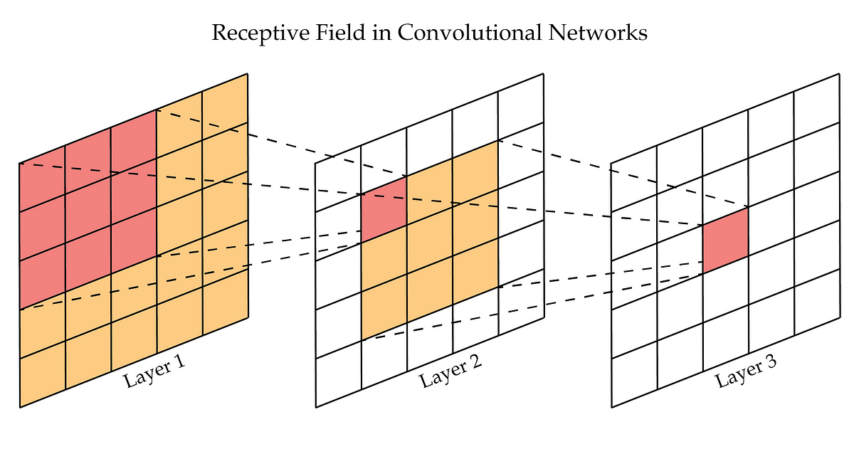
Receptive field: how to make the network see patterns that span more than 3 pixels
In the convolutional neural network, you can think of the receptive field as being all the pixels in previous layers that contribute to one pixel in a deeper layer. The receptive field is a function of the filter size and stride. For example, what this figure shows is that, with a filter size of 3x3, the receptive field of any point in the second layer would be 3x3 pixels; the receptive field of a point in the output layer would be 5x5 pixels; the fourth layer, if shown, would be 7x7; and so on.
With a convolutional autoencoder, downsampling has a huge effect on your receptive field. Every time the image is downsampled by a factor of 2, you double your receptive field. So if you are iteratively downsampling and filtering say, 4 or 5 times, your receptive field becomes very large.
This is very important for reconstruction because many of the shapes and objects you want the network to learn to reconstruct don't just span one or two pixels. There are some kinds of aliasing, like internal texture detail, that do, but other very common sources, like the edges of geometry, can be very large. What this means for DLSS is that removing a downsampling layer doesn't just affect the complexity of the features the network can learn; it also affects the spatial extent over which the network can learn features and do reconstruction.
Why does this matter for Switch-customized DLSSIt matters because it means that the changes you can make to the DLSS architecture have wider ramifications. If you remove one of the downsampling layers, you also have to remove one of the upsampling layers to preserve the symmetry of the network; you also end up reducing the receptive field by a factor of 2, which diminishes DLSS' ability to recognize and reconstruct longer range patterns; and you remove one of the steps in which the network is forced, through downsampling, to make mathematical decisions about which information it needs to preserve for reconstruction.
This means that removing a layer is not just a simple tradeoff, where you can tweak the dimensional knobs of the network a bit to reduce the computational cost. It has major ramifications for the spatial scale of the information you can reconstruct.
So what changes can we make?There are still some options that can make the network a bit lighter. Maybe the easiest way to explain this is to show a few different examples of convolutional autoencoder architectures.
Facebook neural supersampling
This is the architecture from the Facebook neural supersampling paper that we've all discussed quite a bit. The core reconstruction network is a convolutional autoencoder, where you can see some of the features I left out of my "simple convolutional autoencoder" explainer post. In particular:
Deep DIC
- Instead of using stride size and convolution/transpose convolution for downsampling and upsampling, they use pooling and upsampling (from other experience, I believe it's probably max pooling and bilinear upsampling, respectively, but it's not actually mentioned in the paper).
- There are two layers between each downsampling/upsampling step. However, these layers don't violate the "rules" of autoencoders; the encoder never increases in overall dimension, and the decoder never increases in overall dimension. However, having multiple layers does let you somewhat increase the complexity of the features you can learn; in multilayer perceptrons, I once saw a proof that adding an additional layer has a combinatorial effect on the complexity of the functions you can learn. That's the reason that deep learning, with many layers, is more effective than a shallow neural network with one enormous layer, even though the shallow network of an arbitrarily large size can theoretically learn an arbitrarily complex function. But I'm digressing.
- That means you could strip out those "extra" layers between downsampling and upsampling steps if you wanted to reduce computational cost. But like I said, each layer lets the network learn significantly more complex features. It can have a big impact on image quality.
- The Facebook paper also includes an additional network which they refer to as Ours-Fast, which reduces the number of output channels (e.g., the number of learned features) of each layer by 50%, which decreases the total run time from 18.3 ms to 17.2 ms (on a Titan V; this paper is getting old). The image quality does decrease, but is still quite close in structural similarity and PSNR to the full size network (it's Table 3 in the paper, if anyone is checking). This is perhaps the primary optimization that a custom version of DLSS could make.
- The network has skip connections between the input layers and the output layers of the corresponding size. This is because downsampling always removes high frequency information (in the spatial frequency sense). Using skip connections allows the network to only learn the difference (in statistical terms, the residual) between the input and output, preserving high frequency information.
Digital image correlation is to solid mechanics what optical flow is motion in image processing; it tracks the displacement of each particle in a random pattern (think of spray paint) deposited on the surface of a sample and uses them to generate displacement and strain fields. One of the problems in the field is that discontinuities, like cracks in fracture, don't behave very well with DIC. The idea between this Deep DIC paper, which is a collaboration between Northwestern and Ford research, is that you can train a neural network to learn how to reconstruct displacement and strain fields from synthetic (computer generated) DIC data which contains discontinuities.
They train two networks, one for displacement and one for strain. The input to these networks is two images: a reference image and a deformed image. The output for the displacement network has two channels (x and y displacement) and the strain network has three channels (two normal strain components and a shear strain component).
Here are some of the features of this network:
- One layer uses max pooling, but all the others use convolution and deconvolution. The max pooling layer occurs early on to force the network to make a decision about what information to propagate forward.
- Again, we see the symmetry of the encoder and decoder, with skip connections to propagate higher frequency information through the network. This is important because one of the main goals is reconstructing discontinuities, which are always high frequency.
- The network follows the autoencoder rules about dimensions of the encoder always decreasing and the encoder always increasing, except for the last layer of the encoder in the displacement network. It also follows the common convention of always doubling the number of channels and halving the height and width in the encoder, and vice versa in the decoder.
Intel supersampling and denoising
This network is equivalent to DLSS ray reconstruction, doing supersampling and denoising with a single network. I want to make a separate post about this at some point, but I haven't had the time. In particular, it does some really interesting things with its loss function which may explain some aspects of DLSS. But I'll save that for later.
This network is actually several blocks chained together, so it's much more complex. But to summarize the features:
That's a lot of bullet points about the autoencoder portion of the reconstruction. But maybe the most interesting/unusual part of Intel's approach here is the filter paths, which handle reconstruction of specular/diffuse lighting and albedo/normal. This looks like a convolutional network in architecture... but it's not. It might not even qualify as a neural network!
- The input block does an initial projection step (a normal layer without an activation function), then learns some initial features and average pools the output to prepare the input for the feature extractor. There's a skip connection from the input block to the output block to pass through the high frequency information.
- The feature extractor is a version of a convolutional autoencoder, specifically a modified U-Net (which is a standard autoencoder-type architecture in image segmentation). The encoder is shown in blue and the decoder in green. The classic U-Net doubles the number channels with every step in the encoder and halves the number of channels in the decoder; the U-Net has four downsampling steps, so the innermost layer in the encoder ends up with 1024 channels (64 * 2^4).
- From the perspective of DLSS modifications, the most important thing to see is that this feature extractor network no longer simply doubles the number of channels with each downsampling step. The Intel network still downsamples four times, but the innermost layer only has 256 channels, significantly decreasing the computational cost while still maintaining the receptive field and forcing the network, through downsampling in the encoder, to make choices about which information to send through to the decoder for reconstruction. The "basic rule" of an autoencoder, that the dimension of each layer decreases in the encoder and decreases in the decoder, is still followed.
- This is what I mean when I argue that it's unlikely that any modified version of DLSS on the Switch 2 would remove downsampling/upsampling steps. Even in a modified network, these steps are a key feature of the autoencoder. Removing them would have serious ramifications for the output image quality.
- Again, skip connections are used to pass through high frequency information from the encoder to the decoder. This network uses max pooling for downsampling in the encoder and bilinear upsampling in the decoder.
That's a lot more bullet points than I meant to write, but there are so many interesting aspects of this network. I'd really recommend reading the paper to anyone who's interested in how DLSS ray reconstruction works.
- In a convolutional network, filters of a certain size are run over the input from the previous layer. Often, these filters are 3x3, but not always. These same parameters are shared all over the image to pull out relevant features. The weights of these filters are trained during the mathematical optimization of the network.
- The filters in the "filter paths" section of this network are not convolutional. They aren't shared all over the image. They aren't even learned, in the normal sense of machine learning. Here's a verbatim quote from the paper to drive the point home: "there are no learnable parameters in the filter paths."
- Instead, they're per pixel filters over the entire image space which are predicted by the kernel predictor (kernel is another word for filter) as the feature extractor runs. What this means is that, as each layer of the decoder runs, the input for that layer is also filtered by the kernel predictor to get per pixel filter values for every point in the diffuse/specular maps. To me, that's wild! I hadn't seen anything like this before, although they cite papers that have done similar work, so I guess there's a precedent.
- There's still skip connections, and the output of each layer in the network still serves as the input for the next layer. And there's a a ReLU activation function too. So in every sense, the diffuse/specular filters are like a convolutional autoencoder, except that the weights aren't trained or shared across the image.
- The downside of this approach is that, since this isn't convolution, it doesn't map to matrix multiplication in the same way that convolution does. For that reason, Intel runs this part of the network using shaders in Vulcan rather than using TensorRT. Calls to execute the actual neural neural network layers, on the other hand, are handled with TensorRT. Table 4 summarizes how much time is spent on each execution path (4.08 ms in TensorRT and 1.11 ms in Vulcan).
- Albedo/normal are not treated with an autoencoder-like architecture like diffuse/specular are. Instead, per-pixel kernel weights are predicted in the output block. The reason that you would want to use the autoencoder-like architecture is to increase the receptive field and the complexity of the features that you learn; however, the paper claims that you don't need this for albedo/normal. I'm not sure if I'm representing the subtleties of this point well, so here's the direct quote: "We do not predict kernels for auxiliary buffers(albedo and normal) at this stage [during feature extraction], since a large receptive field is not necessary for aliased signals."
- There are some other interesting aspects here about temporal filtering that I need to understand better to write about; I may try to do this another time, when I've spent more time with it. My current understanding is that the current frame and the previous frame, warped with motion vectors, are handled with different filters in some (maybe all?) cases.
- Finally, the filtered specular, diffuse, and albedo are combined into a composite and bilinearly upsampled to the output resolution, then concatenated with the features from the output block, and filtered with another with another per-pixel filter at the output resolution, which generates the output image.
tl;drYeah, me too. This post got way off track. Sorry about that; hope it was interesting! I fucking love this stuff.
The takeaway point, as far as Switch 2 is concerned, is this: convolutional autoencoders are tricky. You can't strip out the downsampling or upsampling layers, because it takes away the main power of a network like this: learning what features matter over a large receptive field.
There are some changes that Nvidia could still make to DLSS for Nintendo, like decreasing the number of channels per layer. But I'm increasingly of the opinion that they won't do this. Whatever the specifics of the DLSS architecture look like, they've been carefully selected by Nvidia to balance all of these considerations. Removing layers or decreasing the number of channels always has downstream effects in a neural network, but in a convolutional autoencoder, they're particularly prevalent.
Honestly, I'm now falling more into the camp that I've seen Oldpuck express before; if there's an issue hitting 4K with DLSS, just have DLSS output to 1440p and then use another upsampling method to get the rest of the way. Maybe I'll be wrong about this! I am 100% sure that the kind of magic, "hardware-optimized" model that some posters seem to expect does not exist, but there are some small tweaks you can make to the architecture to get, perhaps, up to 30-40% more performance. Either way, I hope this post can lead to a conversation that's grounded in the specifics of how a neural network model for this kind of thing works.
We out.
CitationsFacebook neural supersampling: https://research.facebook.com/publications/neural-supersampling-for-real-time-rendering/
Deep DIC: https://www.sciencedirect.com/science/article/pii/S0924013621004349
Intel supersampling denoising: https://www.intel.com/content/www/u...rally-stable-denoising-and-supersampling.html
My previous post about some of the basics of a convolutional autoencoder: https://famiboards.com/threads/futu...-staff-posts-before-commenting.55/post-450982
My post on aliasing vs noise: https://famiboards.com/threads/futu...-staff-posts-before-commenting.55/post-783007
Interesting portable external GPU, mostly meant for more powerful rendering than an integrated GPU. Uses Thunderbolt 4 and/or USB 4.
Storage doesn't really have anything to do with using an eGPU. They generally just care more about how fast you can push data through whatever port they're connected to, though the more pressing issue in a Switch-like device is that they'd probably interfere with the ability to just pull the system out of the dock whenever.I wonder if the high-speed storage solution they're using+the FDE would allow for something like this to be viable on a Nintendo Switch successor, even if it takes a little bit longer for the image to go to the TV. If so, could be used for a Pro.
It looks like Orin supports HDMI 2.1, so I would assume T239 could theoretically support it, just like how a Tegra X1 could support HDMI 2.0, but Nintendo will limit it enough so it supports 4K60 at max, maybe with HDR on top of it as well.Small question...
Based on what we know about the T239... is HDMI 2.1 support a sure thing?
Since all the 2.1 features are officially optional, technically yes.Small question...
Based on what we know about the T239... is HDMI 2.1 support a sure thing?
Just future proofing, mostly.Since all the 2.1 features are officially optional, technically yes.
More seriously, the HDMI chip will be in the dock, which we have no direct information about. If I recall correctly, the SoC supposedly doesn't even have the (disconnected) HDMI interface anymore.
If there's a specific feature this question is a proxy for, it might be more fruitful to ask about that.
4.9TFLOPs. After a certain point getting jumps in TFLOPs requires bigger jumps in Clocks, especially for smaller silicon (So like, if you want to double the 4TFLOPs of 1.3GHz you'd need to hit 2.8GHz)So what does a 1.6GHz clock get you?
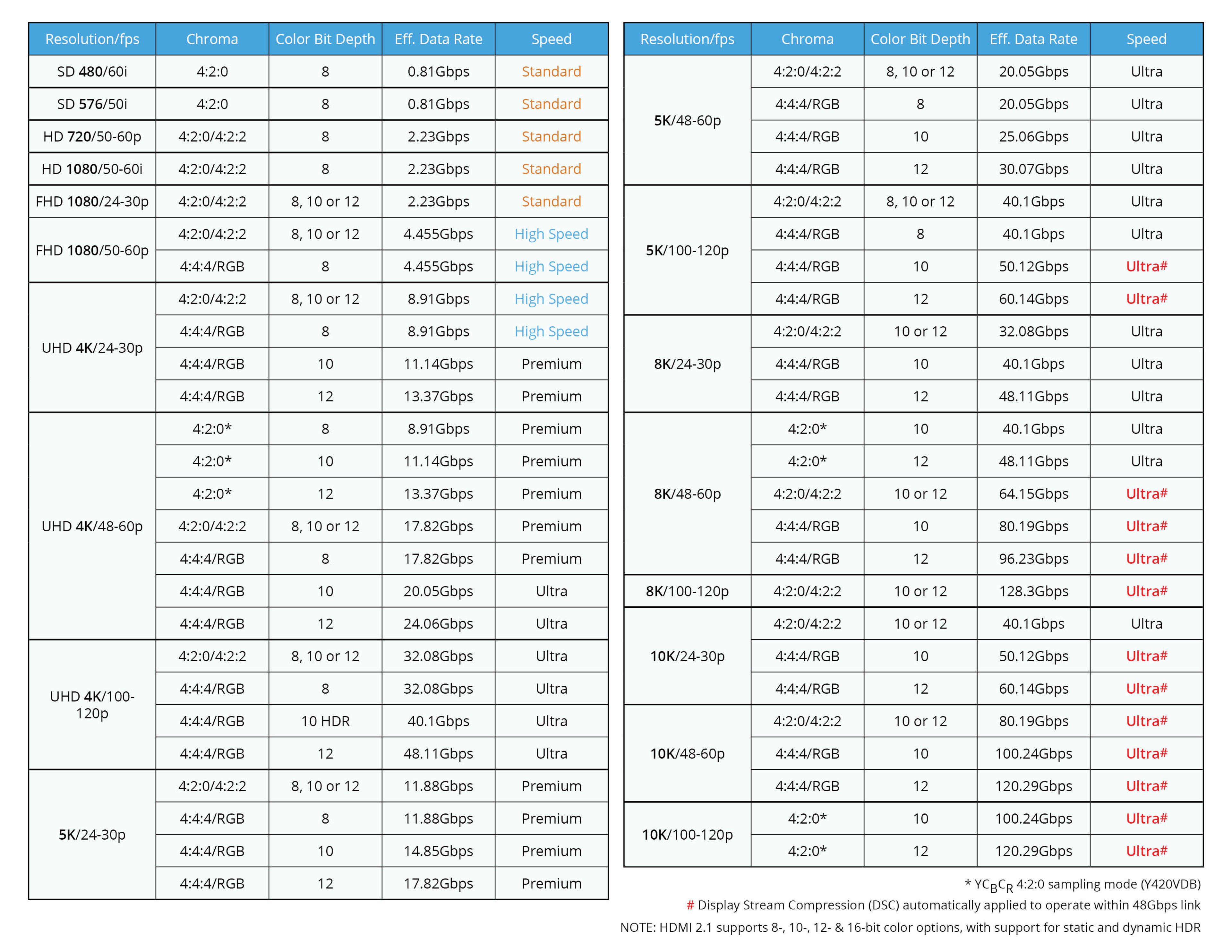
The bolded are going to be limited by DisplayPort 1.4a's max bandwidth of 32.4 Gbps, considering T239 does support DisplayPort 1.4a. And assuming the dock for Nintendo's new hardware supports HDMI 2.1, the dock probably converts the DisplayPort 1.4a signals from T239 to HDMI 2.1 signals via a DisplayPort 1.4a to HDMI 2.1 converter chip (e.g. RTD2173). Display Stream Compression (DSC) is definitely needed for 4:4:4/RGB 10-bit HDR or higher.Just future proofing, mostly.
Support for VRR, eARC, ALLM, Dynamic HDR, 120Hz support at 4K, and stuff like that.
Great post all round. This absolutely isn't my field, so it's great to hear you break it down.Honestly, I'm now falling more into the camp that I've seen Oldpuck express before; if there's an issue hitting 4K with DLSS, just have DLSS output to 1440p and then use another upsampling method to get the rest of the way. Maybe I'll be wrong about this! I am 100% sure that the kind of magic, "hardware-optimized" model that some posters seem to expect does not exist, but there are some small tweaks you can make to the architecture to get, perhaps, up to 30-40% more performance