• Hey everyone, staff have documented a list of banned content and subject matter that we feel are not consistent with site values, and don't make sense to host discussion of on Famiboards. This list (and the relevant reasoning per item) is viewable here.
  • Do you have audio editing experience and want to help out with the Famiboards Discussion Club Podcast? If so, we're looking for help and would love to have you on the team! Just let us know in the Podcast Thread if you are interested!

StarTopic Future Nintendo Hardware & Technology Speculation & Discussion |ST| (Read the staff posts before commenting!)

But I could see it still to be possible to do something like this. Just not for the normal model. Something like a Pro Dock with more power, but protected by a mechanism to enable the switch. Thus you get say PS5 power in Pro Dock, but it always is a few seconds process to do the switch. This would never fly in the mass market version, but people who say, they never play undocked or just want brilliant graphics would accept it.
An external GPU means you have to pay twice for GPU + VRAM + cooling, while adding latency, making things harder to Nintendo and to developers.

A home console + NG Lite would do the same job for about the same price, while being much simpler and cheaper for those who don't want portability.

But even that simply doesn't make much sense over just doing a pro hybrid which boost both portable and docked - even if the docked GPU isn't on par with the PS5. That would still appeal to the docked-only audience willing to pay premium, while also appealing to those who care about portability.
 
0
Oh so it's a dock thing. Probably will provide High Speed HDMI (4K/120FPS).
As I've mentioned below, the bolded is going to be limited by DisplayPort 1.4a's max bandwidth of 32.4 Gbps, considering T239 does support DisplayPort 1.4a.
The bolded are going to be limited by DisplayPort 1.4a's max bandwidth of 32.4 Gbps, considering T239 does support DisplayPort 1.4a. And assuming the dock for Nintendo's new hardware supports HDMI 2.1, the dock probably converts the DisplayPort 1.4a signals from T239 to HDMI 2.1 signals via a DisplayPort 1.4a to HDMI 2.1 converter chip (e.g. RTD2173). Display Stream Compression (DSC) is definitely needed for 4:4:4/RGB 10-bit HDR or higher.

misc-formatdataratetable-large.jpg
Probably DisplayPort Alt Mode 1.0b at best (here and here) if "4kdp_preferred_over_usb30" on system update 12.0.0 is any indication. And I have doubts Nintendo's new hardware is going to support USB4 40 Gbps.
 
Great post all round. This absolutely isn't my field, so it's great to hear you break it down.

I know the "double upscale" gets pooh-poohed a lot but I don't think it's that weird. Games at non-native resolution have been an issue for decades, and are still being produced on the current consoles. But DLSS isn't just an upscaler - it's finding detail that doesn't exist in the native frame. It's more like DLSS is a cheaper path to a reasonable 1440p (or 4k, or 1080p) image, and if the resolution is sufficient, then why not enable more features in that base image?

All that said, I've been messing with a theory that I wanna throw out. Credit to Richard Leadbetter for putting this worm in my head.

Let’s go back to February of last year. Prior to the leak, we were trying to game out what a cut down, Nvidia specific Orin would look like and what hardware could be cut. One of the obvious candidates was the Deep Learning Accelerator, machine learning hardware that seemed useless in a console.

Next month, with the leak in full analysis mode, we discovered Orin’s “double rate” tensor cores. The obvious question is why doesn’t Drake have them. The obvious answer was, at the time, that Nintendo decided that the extra DLSS performance isn’t necessary.

Now, much further out, with additional information, I doubt both of these conclusions.

In the case of the tensor cores, they’re not truly “double rate.” Only a small number of instructions run at double the clock speed. I suspect because these are actually useful for model training, not model execution. That would mean they don’t accelerate DLSS at all, and Nvidia reserves them for their ML products purely for product differentiation.

The DLA is actually well documented, and functions much like tensor cores. They accelerate the same matrix operations as the tensor cores, and in fact, Nvidia’s machine learning tools let you run workloads that combine them into a single compute pool.

I think you’re seeing where this is going. Speculating: DLSS is tensor core limited. Speculating: DLSS can take advantage the of DLA. If so, Nvidia/Nintendo have an option for accelerating DLSS without making the GPU larger than it’s already substantial size.

Initially I thought the DLA was ruled out because it’s not in the list of blocks in the Nvidia driver. But upon review, the block isn’t listed on that place on Orin either. It does show up in other files for Orin, but Drake doesn’t have those files at all - not because the functionality is disabled but because the work was in progress when Nvidia made it private.

Totally speculative, but y’all are smarter than me so I thought I’d throw it out.

The tensor cores on Orin are fully doubled in size. We can see here that all Orin tensor ops are doubled in performance compared to T239 (and desktop Ampere). In particular, the HMMA (FP16) tensor ops which DLSS uses in HDR mode and the IMMA (INT8) tensor ops which DLSS uses in SDR mode are both doubled.

One issue with using the DLA for DLSS is that it seems very heavily tailored to INT8 operations, whereas DLSS's HDR mode (which I believe is the recommended mode which almost every game uses) uses FP16. Although the DLA does support FP16, Nvidia haven't published specifications on FP16 performance anywhere, and the few places it is discussed seem to indicate that it's pretty slow. The answer to this question on Nvidia's developer forums indicates that the Orin DLA is substantially slower than Xavier's DLA in FP16 operations, and Xavier's DLAs are capable of 5 Tflops of FP16 in total (see here), which would put Orin's FP16 DLA performance way behind T239's ~12-13Tflops tensor core FP16 performance.

Another issue is that the DLAs seem to be quite restrictive about what kind of networks they support, which you can see here in the TensorRT docs. They are at least built for convolutional networks like DLSS, but it's possible there are features of DLSS which simply aren't supported by the DLA cores.
 
Given what we know, I'd only safely assume 4K60 HDR10 at 4:2:0 or 4:2:2. I doubt Nintendo has any incentive to push past that, while simplicity and ease of set-up are part of their "brand". They probably don't want people wondering if they have the right set-up to do 120hz, or VRR, or Dolby Vision, and will, at least from where I stand, probably target the "lowest common denominator" of 4K gaming, 4K60 HDR with chroma subsampling. This also fits into the DP1.4a video output T239 sports, as Dakhil points out.
 
It's fucking Saturday. No way they will announce it today or tomorrow.
You could interpret that to mean the next 7 or so days. In my mind, if anything is announced in the next 2 weeks then dude might have had a source.

Then again, I've been on team late Oct (maybe early Nov) announcement for some time, so perhaps that wouldn't validate anything.
 
But I could see it still to be possible to do something like this. Just not for the normal model. Something like a Pro Dock with more power, but protected by a mechanism to enable the switch. Thus you get say PS5 power in Pro Dock, but it always is a few seconds process to do the switch. This would never fly in the mass market version, but people who say, they never play undocked or just want brilliant graphics would accept it.

The dock is gonna be expensive since nearly everything a console need, the dock will need. You will still have the same CPU however so you'll be paying more than a PS5 for less power since even if there's a RTX4090 in the dock, it will be heavily limited by the CPU and bandwidth.
 
The dock is gonna be expensive since nearly everything a console need, the dock will need. You will still have the same CPU however so you'll be paying more than a PS5 for less power since even if there's a RTX4090 in the dock, it will be heavily limited by the CPU and bandwidth.
External GPUs are an option for Nintendo with the Switch format, but it makes more sense to just start with a large GPU and clock it down for handheld mode.

Like, say, T239. 😅
 
You know, i'm in the hunt for an ultrawide monitor for both productivity and gaming, and the more i research, the less i want the Succ to have an OLED screen.

Hell, it has made me wary of the Switch OLED, despite wanting one. The risk of burn in and the lack of a timefram in wich it can happen for sure means to me that it's a technology that isn't ready yet, and it could even be merely transitional before the real deal, whatever it is, actually happens.

Give me a bright IPS screen with a nicely tuned HDR mode and call it a day. I don't want to be looking obsessively for burn in after 6 months, i want to enjoy my Succ without a care in the world.
Switch OLED takes about a year of running the same image to start to burn in. It’s been tested.
 
So I came across a die shot photo of Huawei's Hi36A0 V200 ES chip, which happens to have two Cortex-A78 cores on Twitter.
F65OMaQaEAI8JtL


F65PS8Ba8AA5gCJ

I don't know if Huawei's Hi36A0 V200 ES chip was fabricated using TSMC's N5 process node like with the Kirin 9000.

But if Huawei's Hi36A0 V200 ES chip's indeed fabricated using TSMC's N5 process node, and assuming Drake's fabricated using TSMC's 4N process node, then Huawei's Hi36A0 V200 ES chip should offer a rough idea of how big each Cortex-A78C core is on Drake.
 
Last edited:
The dock is gonna be expensive since nearly everything a console need, the dock will need. You will still have the same CPU however so you'll be paying more than a PS5 for less power since even if there's a RTX4090 in the dock, it will be heavily limited by the CPU and bandwidth.
I've always had this theoretical idea, that I have no idea how not feasible it must be, that you could have a dock that has just the 4080 equivalent or whatever in it, and when docked the handheld turns off all GPU cores which gives extra headroom to allow the CPU to be clocked up, perhaps considerably.

Of course the problem there is I think you want the CPU to be the same in handheld and docked...
 
Dunno where this speculation about Switch NG coming in 2025 started but absolutely NOT
The hardware will not skip 2024 and we'll have before next revisions (or upgrades) for both Xbox Series / PlayStation 5

Switch 1 will remain as focus until the end of this FY, with a decline on it's 'momentum' starting H2 2024
As always, thank you for your input, Necro. It makes sense for this current gen of Switch to decline in H2 of 2024 because it would already be well over a year after the Mario Movie and Tears of the Kingdom. They need something to reinvigorate the Switch brand, and what better than a successor with games you couldn’t play before in your current Switch?

I propose a timeline:
• Holiday period silence over Switch 2
• Switch 1 trailer drop style for the Switch Next Gen after the Fiscal Year ends
• Next month there’s a presentation with First and Third Party content
• Two to three months later, release

That bit about developers and the month of March could be to have marketing material ready for a presentation, like a Direct. A digital presentation. Like:
• Have your Switch 2 running demo ready for when we present the console’s software in lr after March

If 3rd parties have until March to deliver, assuming Nintendo edits it into their format, this could very well take a couple of days, so an event could happen a week or two after. Nevermind outside factors like manufacturing and stuff
 
So I came across a die shot photo of Huawei's Hi36A0 V200 ES chip, which happens to have two Cortex-A78 cores on Twitter.
F65OMaQaEAI8JtL


F65PS8Ba8AA5gCJ

I don't know if Huawei's Hi36A0 V200 ES chip was fabricated using TSMC's N5 process node like with the Kirin 9000.

But if Huawei's Hi36A0 V200 ES chip was fabricated using TSMC's N5 process node, and assuming Drake's fabricated using TSMC's 4N process node, then Huawei's Hi36A0 V200 ES chip should offer a rough idea of how big each Cortex-A78C core are on Drake.

As far as I'm aware the only Huawei chip which was manufactured on TSMC N5 was the original Kirin 9000. US sanctions hit them before phones using the Kirin 9000 hit the market, preventing them from developing any further chips on TSMC's processes. They also had a Kirin 9000E which was a binned version of that chip. They have since developed the Kirin 9000S, on SMIC's "7nm N+2" process, which is used in the Mate 60 Pro.

The puzzling thing is that none of these chips were reported to use the A78 core. The original Kirin 9000 (and 9000E) used four A77 and four A55 cores. The Kirin 9000S uses various cores in the "TaiShan" architecture, which I wouldn't be surprised to find are minor variants on ARM cores, plus four A510 cores.

The leftmost ship above would seem to be the 9000S, and the middle one seems to be the Kirin 9000, which makes the last chip a bit of a mystery. Given the timescale involved in chip tape outs, it's possible that it was the planned successor to the Kirin 9000, which could have taped out just before the sanctions hit. That would explain the rather straight-forward generational upgrades over the 9000 (although the fact that it's apparently precisely the same size as the 9000 is a little suspicious). Very curious indeed.
 
Ok, so I wanted ask my question again but more directly.

LPDDR5 = (128bit / 8 byte * 6400 = 102.40GB/s) (base case)

LPDDR5X = (128bit / 8 byte * 8500 = 136.00GB/s) (reasonable best case)

LPDDR5T = (128bit / 8 byte * 9600 = 153.60GB/s) (never going to happen but would be amazing)

32.8% more bandwidth by using the fastest LPDDR5X

50% more bandwidth using LPDDR5T

Then there is also the possibility they decide to go with 16GB instead of 12GB too

To me these are changes that could easily happen after the Nvidia leak as RAM upgrades often happen later when they get dev feedback

We should stick with 1.1Ghz and 12 GB LPDDR5 as a base case for sure but can someone extrapolate what the best case clock speeds & performance would be given a bandwidth ceiling with 16GB & LPDDR5X?

thanks!
 
I've always had this theoretical idea, that I have no idea how not feasible it must be, that you could have a dock that has just the 4080 equivalent or whatever in it, and when docked the handheld turns off all GPU cores which gives extra headroom to allow the CPU to be clocked up, perhaps considerably.

Of course the problem there is I think you want the CPU to be the same in handheld and ked...

Not feasible at all, Beyond the reasons stated, 4080 starts at $1000 and up. A special dock version only for one machine will cost much more. Even at max possible clock, the CPU would be heavily lopsided. The audience for such a lopsided and expensive console is tiny and not worth the effort and potential confusing marketing losing more audience than you gain
 
Small question...

Based on what we know about the T239... is HDMI 2.1 support a sure thing?
The problem is the output between switch and dock.

The USB-C that switch use can send how much GB/s to the dock? If it's on the range of USB 2.0, then there is no gain in use USB 2.1.
 
The tensor cores on Orin are fully doubled in size. We can see here that all Orin tensor ops are doubled in performance compared to T239 (and desktop Ampere). In particular, the HMMA (FP16) tensor ops which DLSS uses in HDR mode and the IMMA (INT8) tensor ops which DLSS uses in SDR mode are both doubled.
I think what Oldpuck was remembering here was that the consumer Ampere cards appear to have half-rate accumulation of FP16 tensor operations to FP32, specifically, compared to the workstation cards.

In the source code snippets, HMMA_1688_F16_F16 and HMMA_1688_F32_F16 both have the same speed. In Table 3 of the Ampere white paper, which is referring to the A6000 workstation card, this is true; “Peak FP16 Tensor TFLOPS with FP16 Accumulate” and “Peak FP16 Tensor TFLOPS with FP32 Accumulate” both have the same value, 154.8 TFLOPS, like we would expect from the source code.

But if you look at Table 2, which reports the same values for the 3080, “Peak FP16 Tensor TFLOPS with FP32 Accumulate” runs at half the speed of “Peak FP16 Tensor TFLOPS with FP16 Accumulate” (59.5 TFLOPS versus 119 TFLOPS). This happens even though both the 3080 and the A6000 are based on GA102, which is still somewhat mysterious to me.

The source code snippets show that both Orin and Drake would accumulate to F16 and F32 at the same rate, like the workstation cards. I believe that discussion just got mixed up with Orin’s double size tensor cores during all the half-rate/double-rate talk.
 
Last edited:
You could interpret that to mean the next 7 or so days. In my mind, if anything is announced in the next 2 weeks then dude might have had a source.

Then again, I've been on team late Oct (maybe early Nov) announcement for some time, so perhaps that wouldn't validate anything.
Im on team next year. If it's revealed in the very near future, I would be shocked.
 
I think what Oldpuck was remembering here was that the consumer Ampere cards appear to have half-rate accumulation of FP16 tensor operations to FP32, specifically, compared to the workstation cards.

In the source code snippets, HMMA_1688_F16_F16 and HMMA_1688_F32_F16 both have the same speed. In Table 3 of the Ampere white paper, which is referring to the A6000 workstation card, this is true; “Peak FP16 Tensor TFLOPS with FP16 Accumulate” and “Peak FP16 Tensor TFLOPS with FP32 Accumulate” both have the same value, 154.8 TFLOPS, like we would expect from the source code.

But if you look at Table 2, which reports the same values for the 3080, “Peak FP16 Tensor TFLOPS with FP32 Accumulate” runs at half the speed of “Peak FP16 Tensor TFLOPS with FP16 Accumulate” (59.5 TFLOPS versus 119 TFLOPS). This happens even though both the 3080 and the A6000 are based on GA102, which is still somewhat mysterious to me.

The source code snippets show that both Orin and Drake would accumulate to F16 and F32 at the same rate, like the workstation cards. I believe that discussion just got mixed up with Orin’s double size tensor cores during all the half-rate/double-rate talk.

I think that's just an old-fashioned case of artificially limiting functionality on gaming hardware to make the higher-margin professional cards more attractive. The TF32 rate is also halved on consumer Ampere, which makes more sense as I'd expect they would want to push users interested in training onto the pro cards.

Edit: I also suspect both of these are a bit academic, as I would assume DLSS uses FP16 accumulate, and I wouldn't imagine training neural networks is a priority on Switch 2.

That said, I have seen one example of training neural networks in real time for graphics applications, which is Nvidia's Neural Radiance Cache. I don't see any references to the precision used in the paper, but I would guess it's FP16, as quantisation wouldn't be practical for a network that is continually trained and queried. I don't expect NRC to be used in Switch 2 games, but perhaps some developers find other techniques where real-time training is viable.

Also, the section on "Fully Fused Neural Networks" in the NRC paper is quite interesting with respect to the discussion about DLSS. I'd wager they've been using very similar techniques to optimise DLSS for their GPUs.
 
Last edited:
Dunno where this speculation about Switch NG coming in 2025 started but absolutely NOT
The hardware will not skip 2024 and we'll have before next revisions (or upgrades) for both Xbox Series / PlayStation 5

Switch 1 will remain as focus until the end of this FY, with a decline on it's 'momentum' starting H2 2024
this specuation begun due to Furukawa statement on Nikei, stating we gonna suport Nintendo Switch until march 2025, do you really think Nintendo will launch it next hardware considering that?
 
this specuation begun due to Furukawa statement on Nikei, stating we gonna suport Nintendo Switch until march 2025, do you really think Nintendo will launch it next hardware considering that?
They were still supporting the 3DS with software until Summer 2019. Switch 2 being on the market and the OG Switch still getting software support are not mutually exclusive scenarios.
 
But I could see it still to be possible to do something like this. Just not for the normal model. Something like a Pro Dock with more power, but protected by a mechanism to enable the switch. Thus you get say PS5 power in Pro Dock, but it always is a few seconds process to do the switch. This would never fly in the mass market version, but people who say, they never play undocked or just want brilliant graphics would accept it.
This wouldn't fly with game developers, who'd have to spend a lot of extra resources to support a niche scenario.
this specuation begun due to Furukawa statement on Nikei, stating we gonna suport Nintendo Switch until march 2025, do you really think Nintendo will launch it next hardware considering that?
Why would Nintendo wait until they're done making Switch games to launch its successor? They only do that when the older system is already dead or their development teams are in crisis mode.
 
This wouldn't fly with game developers, who'd have to spend a lot of extra resources to support a niche scenario.

Why would Nintendo wait until they're done making Switch games to launch its successor? They only do that when the older system is already dead or their development teams are in crisis mode.
i dont Nintendo Switch to die in the next 2 years, Nintendo will suport Nintendo Switch until year 4/5 of Nintendo next hardware,expect a huge/extended cross-gen period for Nintendo Switch sucessor, dont forget Nintendo want a smooth transiontional period,Nintendo will not end Switch suport in 2025
 
0
thanks for this, I have been lurking on here for a long time and really am here for the hardware speculation
I have a couple questions for you or ideas to think about:

We all know getting too optimistic about Nintendo hardware has been a letdown post the GameCube. That said, we have seen conflicting reports on the amount of RAM that the Switch 2 will have with most people pointing to 12 GB but also some saying 16GB. As far as I understand 16GB is the minimum amount for LPDDR5X and I would also point out that RAM and clock speed profiles are two of the things that Nintendo could absolutely change at the very last minute. We have seen with many consoles including the switch that extra or faster RAM is something that often gets changed after developer feedback.

I guess from a logical standpoint, is it possible for Nintendo to shoot for a higher power advantage in docked mode than you suggest. Just throwing this out there and happy for you, oldpuck or others to shoot this down. With the NVN2, DLSS, known hardware, they could easily go with less standard resolutions for the native rendering and still get clean 1080p and 4k output via DLSS. Perhaps they shoot for something more like 2.5 or 3:1 in terms of the power profiles if they achieved the needed bandwidth with 16GB 8.5 LPDDR5X. Would that potentially provide the overhead for higher docked speeds and thus higher power gap ratio between the two modes?

Would it be a worthwhile tradeoff in handheld mode to be a bit slower than you think sacrificing optimal performance of the chip in favor of passive cooling? This would create quiet gameplay and make hitting the upper end of their battery life goals much more feasible.

You could then introduce a much bigger and quieter active cooling solution via the dock itself which would simply push the air through the device in docked mode allowing for a much higher thermal limit which if we have more bandwidth perhaps could be on the table.

anyways I view all of this as a pie in the sky best case scenario but happy to have it shot down by those that understand hardware better than myself

RAM quantity can change late on in production, but RAM type is something that's nailed down pretty early with the choice of memory controller on the SoC. If T239 has a memory controller which only supports LPDDR5 (like Orin does), then there's no option to change to 5X, as it simply wouldn't work with the SoC. It's possible that they designed T239 with an LPDDR5X controller (they were designing Grace, which supports LPDDR5X, at around the same time), but it would have to have been a very early decision for them.

One reason I'm not expecting LPDDR5X is power consumption. Unlike LPDDR4X, which introduced lower voltages, the 5X standard doesn't do anything to improve power efficiency, which means any increase in bandwidth is going to come with a proportional increase in power consumption. A move from 64-bit LPDDR4 to 128-bit LPDDR5 is already going to result in a jump in power consumption on its own, and it's hard to find good data on the topic, but a rough estimate I made a while ago was doubling from about 1.5W peak on Switch to 3W peak on Switch 2. Moving to LPDDR5X could bring that as high as 4W peak in docked mode, and perhaps 2-3W in portable, which is a lot of extra power they have to account for. Advances in the underlying manufacturing of DRAM might help that a bit (Micron claims an efficiency improvement on their LPDDR5X products), but those same advances could be applied to LPDDR5.

I had speculated a while ago that they may go with a greater than 2x gap in performance between docked and portable modes this time around because of the larger gap in screen resolutions, but I'm not so sure about it now. Part of the reason is the use of DLSS. I fully expect DLSS to be used in both modes, but DLSS doesn't apply quite equally across resolutions, and struggles more at lower resolutions than higher ones. With the same geometry and textures on screen and (let's say) 360p internal resolution scaling to 1080p in portable and 720p scaling to 4K in docked, the DLSS algorithm is going to struggle more on the former, as there's a lot more detail (relative to resolution) for it to decipher. Nintendo probably want to avoid the artefacting that you can get with ultra-low input resolutions in portable mode, whereas using DLSS to push a bit further in docked mode is less likely to cause issues. I'm expecting around 540p-720p internal resolution in portable mode and around 720p-1080p resolution docked, which I think will give closer to "equivalent" image quality in both modes.

I'm also not expecting all games to be pushing 4K in docked mode, even with DLSS. Based on DLSS performance on other Ampere cards, my expectation for a while has been that while 30fps games may hit 4K with DLSS in docked mode, 60fps games are more likely to use DLSS to get to around 1440p. And if you're outputting 1440p docked and 1080p portable, then you're back to around a 2x gap. The reports that the Zelda demo was running at 4K60 via DLSS make me a little more confident that we might get 4K60 games with DLSS, but for the moment my expectations are still somewhere around 1440p after DLSS for 60fps titles (which is still a massive improvement in IQ over the Switch).
 
this specuation begun due to Furukawa statement on Nikei, stating we gonna suport Nintendo Switch until march 2025, do you really think Nintendo will launch it next hardware considering that?
"Supporting Nintendo Switch 1 until March 2025" and "Announcing/Releasing Switch 2 at some point before March 2025" is not mutually exclusive.

Furukawa never said he was going to exclusively support Switch 1 until March 2025.
 
Sorry I mean HDMI 2.0 or 2.1

If the USB on switch can only transfer 5 Gbps, then HDMI 2.0 is the max they can use, no? Since HDMI 2.0 is 18 Gbps.

I read that USB type-C is faster than HDMI 2.0, so, is this not true? Or that is other model?

Display output on Switch (and Switch 2) doesn't use USB signals. It uses the USB C port, but in DisplayPort alt mode, which supports much higher data rates. DisplayPort 1.4a alt mode, which T239 supports, is capable of 32.40 Gbit/s total, or 25.92 Gbit/s when accounting for the overhead of 8b/10b encoding.
 
RAM quantity can change late on in production, but RAM type is something that's nailed down pretty early with the choice of memory controller on the SoC. If T239 has a memory controller which only supports LPDDR5 (like Orin does), then there's no option to change to 5X, as it simply wouldn't work with the SoC. It's possible that they designed T239 with an LPDDR5X controller (they were designing Grace, which supports LPDDR5X, at around the same time), but it would have to have been a very early decision for them.

One reason I'm not expecting LPDDR5X is power consumption. Unlike LPDDR4X, which introduced lower voltages, the 5X standard doesn't do anything to improve power efficiency, which means any increase in bandwidth is going to come with a proportional increase in power consumption. A move from 64-bit LPDDR4 to 128-bit LPDDR5 is already going to result in a jump in power consumption on its own, and it's hard to find good data on the topic, but a rough estimate I made a while ago was doubling from about 1.5W peak on Switch to 3W peak on Switch 2. Moving to LPDDR5X could bring that as high as 4W peak in docked mode, and perhaps 2-3W in portable, which is a lot of extra power they have to account for. Advances in the underlying manufacturing of DRAM might help that a bit (Micron claims an efficiency improvement on their LPDDR5X products), but those same advances could be applied to LPDDR5.

I had speculated a while ago that they may go with a greater than 2x gap in performance between docked and portable modes this time around because of the larger gap in screen resolutions, but I'm not so sure about it now. Part of the reason is the use of DLSS. I fully expect DLSS to be used in both modes, but DLSS doesn't apply quite equally across resolutions, and struggles more at lower resolutions than higher ones. With the same geometry and textures on screen and (let's say) 360p internal resolution scaling to 1080p in portable and 720p scaling to 4K in docked, the DLSS algorithm is going to struggle more on the former, as there's a lot more detail (relative to resolution) for it to decipher. Nintendo probably want to avoid the artefacting that you can get with ultra-low input resolutions in portable mode, whereas using DLSS to push a bit further in docked mode is less likely to cause issues. I'm expecting around 540p-720p internal resolution in portable mode and around 720p-1080p resolution docked, which I think will give closer to "equivalent" image quality in both modes.

I'm also not expecting all games to be pushing 4K in docked mode, even with DLSS. Based on DLSS performance on other Ampere cards, my expectation for a while has been that while 30fps games may hit 4K with DLSS in docked mode, 60fps games are more likely to use DLSS to get to around 1440p. And if you're outputting 1440p docked and 1080p portable, then you're back to around a 2x gap. The reports that the Zelda demo was running at 4K60 via DLSS make me a little more confident that we might get 4K60 games with DLSS, but for the moment my expectations are still somewhere around 1440p after DLSS for 60fps titles (which is still a massive improvement in IQ over the Switch).
Thanks for the info. I also suspect 1440p output resolution to be more common target for ports, with 4K 60 probably either less demanding games or Nintendo flagships. Either way I hope they opt for 16GB of RAM as that will help future proof the system. I would assume everyone here loves Nintendo for their first party games but ultimately the mass market success of Nintendo systems has been much more about reducing the friction for AAA ports.

Outside of RAM and computing power, I really hope we get a much more compelling cart format in terms of speed, cost and size as well as UFS storage expansion solution that is on par with the speed of internal memory. That's obviously a wishlist but it would go a very long way to ensure NG is primed to easily get ports for the life of the console.

Funny how we ended up with better than the best case power scenario from a year ago, but I can't help but want them to boost it more where they can :)
 
0
4.9TFLOPs. After a certain point getting jumps in TFLOPs requires bigger jumps in Clocks, especially for smaller silicon (So like, if you want to double the 4TFLOPs of 1.3GHz you'd need to hit 2.8GHz)

Thus why 1.3GHz is probably the best-case scenario (Which is only really considered at this point because of that appearing in the DLSS Tester profiles. But the 1.1GHz Profile in it and calculated by Thraktor probably are safer to speculate around)
Oh we'll get 1.3 GHz alright. On the modded 3NE chips on the switch 2 revision in 2026/7.

Ok, so I wanted ask my question again but more directly.

LPDDR5 = (128bit / 8 byte * 6400 = 102.40GB/s) (base case)

LPDDR5X = (128bit / 8 byte * 8500 = 136.00GB/s) (reasonable best case)

LPDDR5T = (128bit / 8 byte * 9600 = 153.60GB/s) (never going to happen but would be amazing)

32.8% more bandwidth by using the fastest LPDDR5X

50% more bandwidth using LPDDR5T

Then there is also the possibility they decide to go with 16GB instead of 12GB too

To me these are changes that could easily happen after the Nvidia leak as RAM upgrades often happen later when they get dev feedback

We should stick with 1.1Ghz and 12 GB LPDDR5 as a base case for sure but can someone extrapolate what the best case clock speeds & performance would be given a bandwidth ceiling with 16GB & LPDDR5X?

thanks!
You said before that lpddr5x could only happen/is supported using 16GB RAM (or multiples of 8). That's actually not the case. Unless there is context I'm missing, Both Samsung S23 and Pixel 8 Pro supports 12GB LPDDR5X vs the base models supporting 8GB LPDDR5X.

One reason I'm not expecting LPDDR5X is power consumption. Unlike LPDDR4X, which introduced lower voltages, the 5X standard doesn't do anything to improve power efficiency, which means any increase in bandwidth is going to come with a proportional increase in power consumption
There's only a 20% decrease in power consumption from lpddr5 to x variant. A lot less than lpddr4 to lpddr4x. If they go with lpddr5x, they might as well go beyond lpddr5 clocks.

I'm not expecting 5x either but I'm guessing they could go with 88GB/s in handheld and up to 134GB/s in docked, if we get 5x. 88GB/s to help save on power draw and could be enough for PS4 ports in 1080p maybe. The gap in RAM between modes will be much better than OG switch.

But if it's 88 and 102, it's gonna be bizarre. They could go lower to 68GB/s, but imo only makes sense on a 720p a screen. But we have DLSS though...
 
Last edited:
Oh we'll get 1.3 GHz alright. On the modded 3NE chips on the switch 2 revision in 2026/7.


You said before that lpddr5x could only happen/is supported using 16GB RAM (or multiples of 8). That's actually not the case. Unless there is context I'm missing, Both Samsung S23 and Pixel 8 Pro supports 12GB LPDDR5X vs the base models supporting 8GB LPDDR5X.


There's only a 20% decrease in power consumption from lpddr5 to x variant. A lot less than lpddr4 to lpddr4x. If they go with lpddr5x, they might as well go beyond lpddr5 clocks.

I'm not expecting 5x either but I'm guessing they could go with 88GB/s in handheld and up to 134GB/s in docked, if we get 5x. 88GB/s to help save on power draw and could be enough for PS4 ports in 1080p maybe. The gap in RAM between modes will be much better than OG switch.

But if it's 88 and 102, it's gonna be bizarre. They could go lower to 68GB/s, but imo only makes sense on a 720p a screen. But we have DLSS though...
thanks there must be a difference between what you can query on the Samsung website and what bulk players can order because I only saw 16GB & up

134 & 88 as the two profiles would be great

any idea what the cost difference would be for Nintendo to go with 12GB 5 vs 12GB 5x?

Assuming the T239 can handle 5x... I would think cost would be the main hurdle since they can down clock in portable as you pointed out
 
We should stick with 1.1Ghz and 12 GB LPDDR5 as a base case for sure but can someone extrapolate what the best case clock speeds & performance would be given a bandwidth ceiling with 16GB & LPDDR5X?
@Thraktor explained why we feel like we're stuck with the bandwidth limits of LPDDR5, but figured I'd step in and answer your question directly. Note - this is all @Look over there's work, I'm just recapping.

All of the RTX 30 cards float around 30 GB/s of memory bandwidth for every TFLOP of performance. So in order to perform in the same ballpark as an RTX 30 card, the GPU needs that much bandwidth.

In a console, the CPU and the GPU share a memory bus, unlike PCs. This has performance advantages, but means you will need extra bandwidth for the CPU. CPU performance will need to keep up with GPU performance, generally, so a 20% premium is a good estimate.

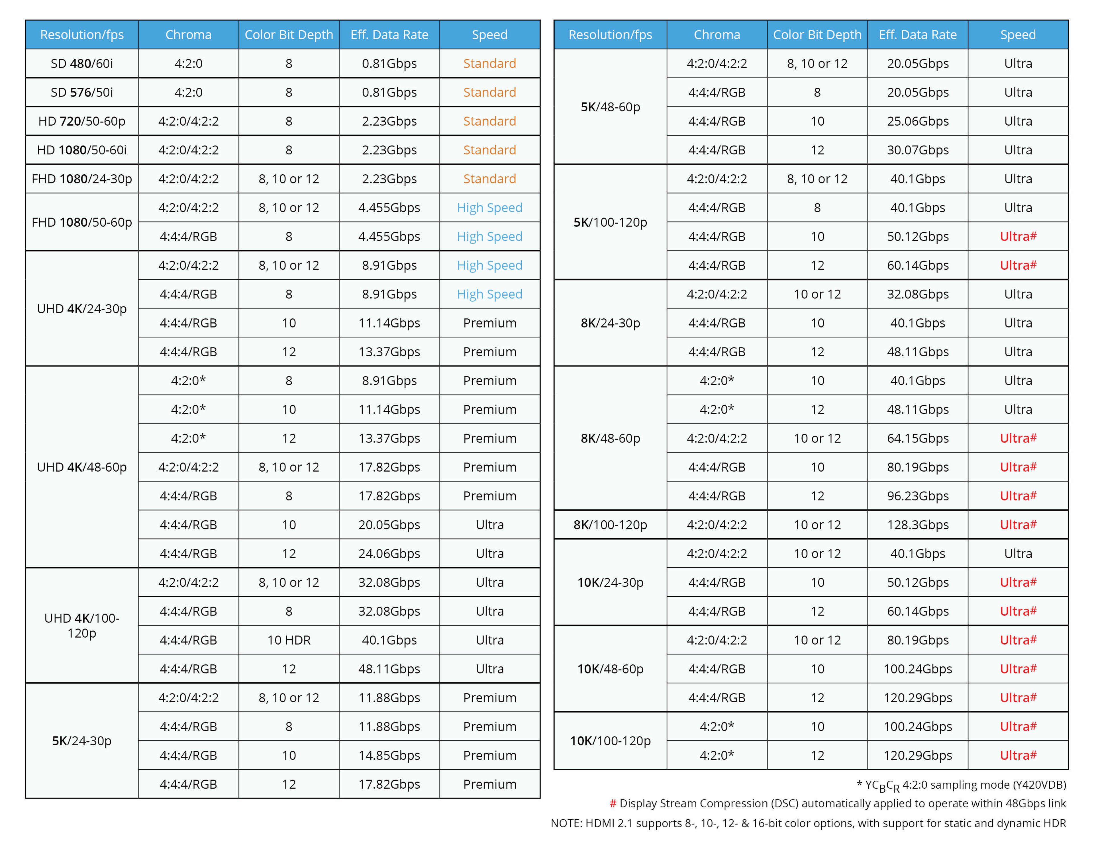
That's the origin of the 3 TFLOP limit. 30 GB/s * 3 TFLOPS * 1.2 = 108GB/s, just a touch higher than the 102 GB/s that would be the max for LPDDR5.

There are some caveats.

First, obviously, not all RTX 30 cards go as high as 30GB/s/TFLOP. The highest end (RTX 3090 Ti) and the lowest end (RTX 3050) both hit 25 GB/s. That may seem unintuitive, but think of it this way. The highest end card is about pushing as much performance as possible. Extra TFLOPS past the bandwidth limit aren't useless they're just less useful. The 3090 Ti is a waste of electricity and money, delivering only marginal improvements for it's huge cost premium, but it's a card targeted at the "fuck it, I don't care, card go brrr" market.

The low end card is sort of the same situation. More bandwidth costs money. The physical silicon is cut down till it hits the cost Nvidia wants, but pushing the GPU clock speed (and thus the TFLOPS) is basically free. So even if those TFLOPS aren't delivering as many frames/pixels as they should, they're still good performance for the $$$.

Nintendo is slightly more constrained. Electricity matters a lot more. Every little bit of electricity spent costs battery life. It also means a bigger heat sink, and a bigger fan, which increases the size and the cost of the device, makes it more expensive to ship, and perversely leaves less room for the battery.

We know a little bit about Nintendo's hardware development process - it's a back and forth between the hardware team and the lead software teams. Software wants more performance, more features. Hardware wants to cut costs and hit battery life targets. When software hits a bottleneck, they ask for more power, when hardware hits a bottleneck they try to cut it.That's why we tend to assume that things will land in the area of best balance and peak efficiency. Because that's the place where the Performance that software wants is the cheapest for Hardware to deliver.

But it's possible that software just Needs More Power, and Hardware has to bite the bullet, and push past the bandwidth limit (like Nvidia did on the low end 3050). It's also possible that, while laying out the rest of the design, there are a few spare milliwatts in the budget, and the biggest bang for the buck is to push the GPU clocks a bit, rather than horde it for an extra 10 minutes of battery life (ala the 3090 Ti).

Of course that could also be true for the CPU clocks, or the storage speeds, or the screen brightness, or the WiFi speed or... so even if this situation occurs, that doesn't mean it's reflected in the GPU clocks. A lot of discussion in the past here has been about whether the T239 is more likely to be limited by the GPU, or the CPU, or the memory bus, or the the storage speed, or even the RAM. The fact that there hasn't been a clear consensus on any of those things is a good sign - it means that T239's design seems pretty balanced.

I tend to fall in the camp of "Nintendo went with a big design. Underclocking it would be wasteful, but it's so big that pushing the clocks isn't required either." I think if there is any wiggle room in the design, Nintendo will spend it making the device smaller, and improving battery life.
 
Isn’t T239 based on Odin which only supports LPDDR5?

Also if it’s based on it, why is the GPU architect so different? (Thinking mainly Tensor cores and RT cores)

Isn’t it directly based on the desktop GPU’s?
 
Display output on Switch (and Switch 2) doesn't use USB signals. It uses the USB C port, but in DisplayPort alt mode, which supports much higher data rates. DisplayPort 1.4a alt mode, which T239 supports, is capable of 32.40 Gbit/s total, or 25.92 Gbit/s when accounting for the overhead of 8b/10b encoding.
So, enough to run 4K at 120fps, if, for example, Microsoft want to port Orin 2 at 120 fps, like the Series S, to Switch 2, right?

When I consult on Bard, these are the number it give me:

4K60 fps14,4 Gbps
4K120 fps23,8 Gbps
8K60 fps33,6 Gbps
8K120 fps67,2 Gbps

But, since it is a AI, I can't trust if it is wright or not.
Normally when Bard give results, it's also supposed to provide clickable footnotes/citations for a human to click through and verify Bard's results etc. Are you not seeing that with those results (the footnotes)?
 
Ok, so I wanted ask my question again but more directly.

LPDDR5 = (128bit / 8 byte * 6400 = 102.40GB/s) (base case)

LPDDR5X = (128bit / 8 byte * 8500 = 136.00GB/s) (reasonable best case)

LPDDR5T = (128bit / 8 byte * 9600 = 153.60GB/s) (never going to happen but would be amazing)

32.8% more bandwidth by using the fastest LPDDR5X

50% more bandwidth using LPDDR5T

Then there is also the possibility they decide to go with 16GB instead of 12GB too

To me these are changes that could easily happen after the Nvidia leak as RAM upgrades often happen later when they get dev feedback

We should stick with 1.1Ghz and 12 GB LPDDR5 as a base case for sure but can someone extrapolate what the best case clock speeds & performance would be given a bandwidth ceiling with 16GB & LPDDR5X?

thanks!

RAM quantity can change late on in production, but RAM type is something that's nailed down pretty early with the choice of memory controller on the SoC. If T239 has a memory controller which only supports LPDDR5 (like Orin does), then there's no option to change to 5X, as it simply wouldn't work with the SoC. It's possible that they designed T239 with an LPDDR5X controller (they were designing Grace, which supports LPDDR5X, at around the same time), but it would have to have been a very early decision for them.

One reason I'm not expecting LPDDR5X is power consumption. Unlike LPDDR4X, which introduced lower voltages, the 5X standard doesn't do anything to improve power efficiency, which means any increase in bandwidth is going to come with a proportional increase in power consumption. A move from 64-bit LPDDR4 to 128-bit LPDDR5 is already going to result in a jump in power consumption on its own, and it's hard to find good data on the topic, but a rough estimate I made a while ago was doubling from about 1.5W peak on Switch to 3W peak on Switch 2. Moving to LPDDR5X could bring that as high as 4W peak in docked mode, and perhaps 2-3W in portable, which is a lot of extra power they have to account for. Advances in the underlying manufacturing of DRAM might help that a bit (Micron claims an efficiency improvement on their LPDDR5X products), but those same advances could be applied to LPDDR5.

I had speculated a while ago that they may go with a greater than 2x gap in performance between docked and portable modes this time around because of the larger gap in screen resolutions, but I'm not so sure about it now. Part of the reason is the use of DLSS. I fully expect DLSS to be used in both modes, but DLSS doesn't apply quite equally across resolutions, and struggles more at lower resolutions than higher ones. With the same geometry and textures on screen and (let's say) 360p internal resolution scaling to 1080p in portable and 720p scaling to 4K in docked, the DLSS algorithm is going to struggle more on the former, as there's a lot more detail (relative to resolution) for it to decipher. Nintendo probably want to avoid the artefacting that you can get with ultra-low input resolutions in portable mode, whereas using DLSS to push a bit further in docked mode is less likely to cause issues. I'm expecting around 540p-720p internal resolution in portable mode and around 720p-1080p resolution docked, which I think will give closer to "equivalent" image quality in both modes.

I'm also not expecting all games to be pushing 4K in docked mode, even with DLSS. Based on DLSS performance on other Ampere cards, my expectation for a while has been that while 30fps games may hit 4K with DLSS in docked mode, 60fps games are more likely to use DLSS to get to around 1440p. And if you're outputting 1440p docked and 1080p portable, then you're back to around a 2x gap. The reports that the Zelda demo was running at 4K60 via DLSS make me a little more confident that we might get 4K60 games with DLSS, but for the moment my expectations are still somewhere around 1440p after DLSS for 60fps titles (which is still a massive improvement in IQ over the Switch).

If I recall correctly didn’t someone (@oldpuck ?) say a while ago that LPDDR5 had recently been shrunk to a more efficient node? And that 5X is just an overclocked 5? So if 5 is now more efficient, and 5X is just a fancy overclock, can we expect anything different in clock speeds on a standard LPDDR5?

EDIT @Dakhil beat me to it. 🤣 Didn’t all 5 production move to that new node as well?
 
Isn’t T239 based on Odin which only supports LPDDR5?

Also if it’s based on it, why is the GPU architect so different? (Thinking mainly Tensor cores and RT cores)

Isn’t it directly based on the desktop GPU’s?
1. I would assume it inherits the memory controller from Orin, but it's a possibility they added lpddr x support.

2. Drake is made by the same team as Orin. Obviously a self driving car, and a gaming consoles are two completely different things, and yes Drake is more like the desktop gpus. It also has the fde, that's neither from desktop or Orin. But it's an arm chip like Orin, there's definitely some things that makes sense to use from Orin.

3. It's a custom soc, made by the Orin team.
 
0
So if 5 is now more efficient, and 5X is just a fancy overclock, can we expect anything different in clock speeds on a standard LPDDR5?
Depends on which RAM controller and RAM modules are being used.

Assuming a LPDDR5 controller and LPDDR5X modules are used, the answer is no, since the LPDDR5 controller caps the max I/O rate at 6400 MT/s, which corresponds to a max frequency of 3200 MHz. And I imagine the answer's going to stay the same, assuming a LPDDR5X controller and LPDDR5 modules are being used, except the reason is because of the RAM modules, not the RAM controller.
 
Last edited:
This has been covered by different posts but in an effort to simplify the GPU series for T239:

Saying it is Lovelace or Ampere is actually a total misnomer... when you are dealing with a custom piece of silicon like T239 you aren't necessarily either. This is exactly what we saw with PS5 & XSX having some features that weren't yet in retail RDNA AMD cards, missing others and even customizations like the geometry engine Cerny used.

The most likely scenario is T239 SMs are based on Ampere on a more efficient node with some learnings/features from Lovelace. Grace Hopper was taping at the same time so perhaps that even had some influence on the design, although unlikely. I am not trying to claim T239 will be anything Grace Hopper, what I am saying is Nvidia would consider pitching Nintendo on features or design tweaks from the cutting edge if they make sense for a lower power device.

When you combine the above with fixed hardware, NVN2 from the ground up with T239 and the DLSS advantage... I suspect whatever the final specs are, this device is going to seriously punch above it's weight. We are hearing exactly that from demo leaks and I can't wait for some hard details to surface.
 
Depends on which RAM controller and RAM modules are being used.

Assuming a LPDDR5 controller and LPDDR5X modules are used, the answer is no, since the LPDDR5 controller caps the max I/O rate at 6400 MT/s, which corresponds to a max frequency to 3200 MHz. And I imagine the answer's going to stay the same, assuming a LPDDR5X controller and LPDDR5 modules are being used, except the reason is because of the RAM modules, not the RAM controller.
yeah did nintendo upgrade the controller since LPDDR5X would have been known to give themselves optionality?

if they did the above, now that they have been testing the SOC would the additional boost in bandwidth make sense from a cost and performance standpoint?

there is a chance the cost is a problem, there is a chance the extra bandwidth doesn't matter due to thermal or other performance bottlenecks

to your point, if they never upgraded the controller the debate ends there
 
0
So I came across a die shot photo of Huawei's Hi36A0 V200 ES chip, which happens to have two Cortex-A78 cores on Twitter.
F65OMaQaEAI8JtL


F65PS8Ba8AA5gCJ

I don't know if Huawei's Hi36A0 V200 ES chip was fabricated using TSMC's N5 process node like with the Kirin 9000.

But if Huawei's Hi36A0 V200 ES chip's indeed fabricated using TSMC's N5 process node, and assuming Drake's fabricated using TSMC's 4N process node, then Huawei's Hi36A0 V200 ES chip should offer a rough idea of how big each Cortex-A78C core is on Drake.

I saw a 2D Metroid map at first.

I need help.
 
Depends on which RAM controller and RAM modules are being used.

Assuming a LPDDR5 controller and LPDDR5X modules are used, the answer is no, since the LPDDR5 controller caps the max I/O rate at 6400 MT/s, which corresponds to a max frequency of 3200 MHz. And I imagine the answer's going to stay the same, assuming a LPDDR5X controller and LPDDR5 modules are being used, except the reason is because of the RAM modules, not the RAM controller.
So the only thing we’re guaranteed is a more efficient RAM versus older devices using 5 RAM on the previous node. Silver lining I guess. 🤷‍♂️
 
0
And LPDDR5X having 20% better power efficiency than LPDDR5 comes purely from using a newer process node (Samsung's 1z (15 nm*) process node for LPDDR5 vs Samsung's 14 nm* process node for LPDDR5X).
* → a marketing nomenclature used by all foundry companies
That's interesting.

Apparently Micronix offers 24%. Slightly more than Samsung.

thanks there must be a difference between what you can query on the Samsung website and what bulk players can order because I only saw 16GB & up

134 & 88 as the two profiles would be great

any idea what the cost difference would be for Nintendo to go with 12GB 5 vs 12GB 5x?

Assuming the T239 can handle 5x... I would think cost would be the main hurdle since they can down clock in portable as you pointed out
I'm not sure about the cost difference. But I think it would be significant enough for Nintendo to choose 5 over 5x, if they wanted to save money. RAM is one of the most expensive components of PC hardware and consoles.
 
0
Normally when Bard give results, it's also supposed to provide clickable footnotes/citations for a human to click through and verify Bard's results etc. Are you not seeing that with those results (the footnotes)?
No, I'm not. There is a option to "search on google", but that is it.
 
0
this specuation begun due to Furukawa statement on Nikei, stating we gonna suport Nintendo Switch until march 2025, do you really think Nintendo will launch it next hardware considering that?
why is it that in this thread, routinely I feel, things are said that don’t have source or never happened and are pushed to be fact😭

Like when did he say this, let’s bffr 😹
 
why is it that in this thread, routinely I feel, things are said that don’t have source or never happened and are pushed to be fact😭

Like when did he say this, let’s bffr 😹
He literally said that. But it's meaningless re: successor timing.

If the successor launched RIGHT NOW, first party Switch support ending by end of March 2025 would give Switch 1 shorter post-succssor support cycle than GBA, DS, or 3DS. If they're serious about that March 2025 deadline for first party Switch 1 games, holy hell, we're in for a VERY fast turnaround for reveal to release and a VERY early 2024 release, because less than 1 year of crossover is downright ill-advised.
 
Please read this staff post before posting.

Furthermore, according to this follow-up post, all off-topic chat will be moderated.
Last edited:


Back
Top Bottom