
Dark Cloud
Warpstar Knight
iMessNot sure why, but in all this excitement I find myself wishing iNess was around to drop some barely comprehensible ramblings to really bring things up a level.
iMessNot sure why, but in all this excitement I find myself wishing iNess was around to drop some barely comprehensible ramblings to really bring things up a level.
How much more the main PS5 unit cost vs the Digital version in your opinion ?The second SKU would cost like $20 more to produce, lol.

Who said their source on display type was a developer? They don't make that distinction.
You're right that the upgrade to OLED shouldn't be that much more, but the VGC article directly states why their sources think nintendo would be desperate enough to cut corners on some stuff: to offset costs from increased internal storage/memory costs.Not really? OLED screens are like $5 to $10 more at this point and don't have a different form factor (like the XL).
Well here's Nintendo's carefully worded response to what Mochizuki had claimed...
Yes hindsight is 20/20 and we now know that the OLED has a partial metal frame, so that definitely would increase the build price.
We still don't know how much the OLED displays run Nintendo but it would be a downgrade them going back to LCD.
Short version: no, it will not be out of dateHere's a question for the tech-heads from someone who is primarily concerned with this thing's capabilities as a home console box.
My understanding is that Drake has been "taped out" and awaiting production for ages - over a year (if I recall correctly). So if Switch 2 with Drake releases in late 2024, will developing Drake when they did have been a mistake? Will the SoC be out of date versus what they could have done had they waited a year or two?
Slightly longer version - tech moves way way slower than most people image. There are basically no major improvements in the design of GPUs or CPUs in the last 5 years - plenty of minor improvements, but nothing huge.Or has mobile / Tegra / whatever tech not progressed that much in the interim?
Okay, let's make a distinction here that will help. "Drake" is the name of the chip that is in the Next Generation Switch. Switch 2 (or SwitchNG or redacted, or whatever the hell you wanna call it) is the console made with that chip. "Van Gogh" is the name of the chip in the Steam Deck.I've just read a lot about Drake probably being slightly weaker than a Steam Deck, and while I know that a locked-in console dev environment will offer all kinds of gains and advantages it still seems lame to be getting that a full two and a half years after the deck's original release in Feb 2022. (Which is what prompts the question)
I don't think there's danger of that. I think it's questionable whether we'll see as many cartridge based games going forward on the Switch 2.All I know is that backwards combability is a must, I know Furukawa mentioned that they want a smooth transition between the switch and it's successor with the use of Nintendo Account Online. It would be a shamed that if I can't play all the digital games I purchased on my switch on the NG Switch...it's been a big weakness since the Wii to Wii U days which was a pain when they made you rebuy your VC console games (at a discounted price if you transfer your wii data) just to play them on the Wii U.
You're talking about two different companies with two completely different approaches to hardware.Or they could do OLED and possibly just lose a little each console like Sony does
How much more the main PS5 unit cost vs the Digital version in your opinion ?
well Switch launched with a chipset, a lot of people considered outdated, very likely that Nintendo launch the Switch sucessor in 2024 or even 2026Early 2024 (Arguing Nintendo's tendency to not have products in full production for too long in order to avoid factory leaks)
VS
Late 2024 (Fully believing the article and that Nintendo would let a product stay in full production for around/over a year)
VS
2025 (People who think Modern Nintendo, the guys putting a GPU way bigger than anyone expected in this thing, would really be fine letting a SoC with 2022 (arguable best) tech come out in 2025 running a 5-year-old Architecture on CPU and GPU)
I know it's not happening I literally said that in another postYou're talking about two different companies with two completely different approaches to hardware.
Idk what to tell you besides that's probably not happening.
Well here's Nintendo's carefully worded response to what Mochizuki had claimed...
Yes hindsight is 20/20 and we now know that the OLED has a partial metal frame, so that definitely would increase the build price.
We still don't know how much the OLED displays run Nintendo but it would be a downgrade them going back to LCD.
Based on Nvidia's roadmap, it'd be at least another year or two before they'd have a significantly better architecture in general, and Tegras tend to lag behind a bit. In principle, they might have been able to get a few more of the Lovelace changes had they waited a bit longer, but they're probably not in a significantly worse position than they were with Switch and Pascal.Here's a question for the tech-heads from someone who is primarily concerned with this thing's capabilities as a home console box.
My understanding is that Drake has been "taped out" and awaiting production for ages - over a year (if I recall correctly). So if Switch 2 with Drake releases in late 2024, will developing Drake when they did have been a mistake? Will the SoC be out of date versus what they could have done had they waited a year or two? Or has mobile / Tegra / whatever tech not progressed that much in the interim?
I've just read a lot about Drake probably being slightly weaker than a Steam Deck, and while I know that a locked-in console dev environment will offer all kinds of gains and advantages it still seems lame to be getting that a full two and a half years after the deck's original release in Feb 2022. (Which is what prompts the question)
I've heard stuff, yes.Would you happen to know anything on this particular subject? A yes or no would suffice :]
Not having an OLED would be pretty shite. I didn’t get the impression that the OLED screen specifically was why the Switch OLED cost more. There were quite a few other changes to the construction, so while Nintendo did deny the claim around the BOM, I don’t remember anything conclusive about OLED screen prices?
LCD is a downgrade in terms of color accuracy usually and the blacks are unmatched and I could be wrong on all of this but I think pixel response times are better on OLED as well and it's better for battery although I think it's such a small amount of battery actually being saved it's within the realm of testing discrepancyLCD is not a downgrade, OLED is much more expensive and risk your display of burn-in, i would be extremely/more worried for lact of backward compatibility then OLED display on Nintendo next gen hardware, dont you all realize OLED was only meant for the Switch Pro that became Switch OLED.
Omg Nate confirmed OLED screen for the Switch 2!! I have so many YouTube videos to make today. /sI've heard stuff, yes.
Counterpoint, Tegra X1 in terms of the mobile space was pretty cutting-edge even when Switch came out.well Switch launched with a chipset, a lot of people considered outdated, very likely that Nintendo launch the Switch sucessor in 2024 or even 2026
The only thing about the TX1 that was arguably disappointing was the process node. If they had launched with Mariko and clocked it accordingly it would have been more or less the best chip they could have used.Counterpoint, Tegra X1 in terms of the mobile space was pretty cutting-edge even when Switch came out.
The Snapdragon 810 was pretty much a TX1 CPU wise with it's 4 LITTLE cores engaged....and a WAAAAAAAAAAAAAAAAAY weaker GPU when looking at hardware at TX1's release
And Switch is pretty much all but confirmed to have been pushed out of 2016 due to wanting BOTW specifically finished.
Even in 2016, the mobile flagship for Android to compare against would be the Snapdragon 820....which had rampant overheating issues due to the Kryo Architecture falling flat so hard on Gen1 they backtracked to make a tweaked version of the A73s and A53s for the Kryo 2nd Gen cores versus something custom for the 835 in 2017.
And ARM SoCs were kind of limited still to 4GB even in 2016 so memory couldn't be improved with 2016 technology in the ARM Space.
So the literal only real benefit they could've done for TX1 due to it already sort of running a Pascal-Maxwell hybrid was swap in A72s for the CPU cores. Which, while apricated, wouldn't majorly upend the situation TX1 ended up in. Just let it limp a bit more on CPU limited situations.
People can want both backwards compatibility and an OLED screen. I don't know about as a whole, but between the Switch LCD and Switch OLED screens... I'd take the OLED any day, it's felt like a night and day difference since I upgraded. I'd feel really disappointed if the Switch successor had an LCD screen unless it's a significant step up over the current Switch's.LCD is not a downgrade, OLED is much more expensive and risk your display of burn-in, i would be extremely/more worried for lact of backward compatibility then OLED display on Nintendo next gen hardware, dont you all realize OLED was only meant for the Switch Pro that became Switch OLED.
Bad faith reporting. VGC has form and history for this, ESPECIALLY with regard to Nintendo reporting. Much of what’s been said there is an educated calculation, but all of it is nothing anybody needs to take seriously. EVER. Truthfully, it should be a banned publication for their misinformation at this point.Both PS5 and Series X have the same “issue” of legacy (PS4/One) support that could theoretically affect sales of the current-gen versions. Why is it suddenly a problem with Nintendo?
Or maybe it's just the people hyper focusing on the negative parts.Bad faith reporting. VGC has form and history for this, ESPECIALLY with regard to Nintendo reporting. Much of what’s been said there is an educated calculation, but all of it is nothing anybody needs to take seriously. EVER. Truthfully, it should be a banned publication for their misinformation at this point.
BC has been confirmed for at least nine years, when Iwata was still here. We’ve also seen slides which point to it, and Miyamoto has pointed to it, too, but you have certain Youtwitch grifters with podcasts planting seeds of concern into the discourse. I keep coming back to the fact believing there won’t be BC requires you to believe Nintendo and Nvidia made colossal oversights when entering a long-term partnership. Some people actually believe that, and some influencers with huge followings entertain it “Because Nintendo”, as if that’s a premise at all (It isn’t. It’s a certain way to get blocked over here, tbqh).
Omg Nate confirmed OLED screen for the Switch 2!! I have so many YouTube videos to make today. /s
Short version: no, it will not be out of date
Slightly longer version - tech moves way way slower than most people image. There are basically no major improvements in the design of GPUs or CPUs in the last 5 years - plenty of minor improvements, but nothing huge.
What's changed over those 5 years is the process node - how small you can make a chip. Almost everyone here expects that Nvidia and Nintendo will use TSMC 4N, basically the most advanced process node currently available.
Looking at the "minor" improvements that Drake doesn't have, even those are fairly small on the ground.
Okay, let's make a distinction here that will help. "Drake" is the name of the chip that is in the Next Generation Switch. Switch 2 (or SwitchNG or redacted, or whatever the hell you wanna call it) is the console made with that chip. "Van Gogh" is the name of the chip in the Steam Deck.
Drake has more CPU cores, GPU cores, and a more advanced process node than Van Gogh. However, basically no one expects Nintendo to opt to used as much electricity as the Steam Deck, or to build a device that phsycially huge, with it's giant battery and huge cooling system. So we're all betting that Nintendo will take some of those advantages in Drake and use them to make a powerful device, but hit a limit where they instead spend the rest of those advantages on making a small device with decent battery life
A second distinction - the "slightly weaker than Steam Deck" mostly comes from trying to compare apples to apples. The Steam Deck doesn't have a real "docked" mode, so we're comparing the estimated Switch 2 handheld mode to Steam Deck. Plugged up to the TV, I would expect it to exceed the Steam Deck by a comfortable margin, even being super conservative.
And even then a Switch that launched with Mariko likely wouldnt benefit much from higher clocks as we can tell with Mariko Overclocking. Yeah it's better, but not revolutionary.The only thing about the TX1 that was arguably disappointing was the process node. If they had launched with Mariko and clocked it accordingly it would have been more or less the best chip they could have used.
Thank you!
Why does almost everyone here expects that Nvidia and Nintendo will use TSMC 4N (instead of Samsung 8nm process, the ‘default’ one for T234 Orin) ?
Can it be some confirmation bias because we think more like a Nintendo enthusiast than Furukawa the business decision maker?
(It reminds me when we thought Nintendo will use Tegra X2 for NX)
The cpu could have been close to twice as powerful. Which would have really helped porting from other consoles.And even then a Switch that launched with Mariko likely wouldnt benefit much from higher clocks as we can tell with Mariko Overclocking. Yeah it's better, but not revolutionary.
Mainly due to sheer laws of space and thermodynamics for a device of Switch form factor.Thank you!
Why does almost everyone here expects that Nvidia and Nintendo will use TSMC 4N (instead of Samsung 8nm process, the ‘default’ one for T234 Orin) ?
Can it be some confirmation bias because we think more like a Nintendo enthusiast than Furukawa the business decision maker?
(It reminds me when we thought Nintendo will use Tegra X2 for NX)
My guess is currently 1.7 Tflops in portable mode (12 SMs @ 550MHz) and 3.4 Tflops docked (12 SMs @ 1.1GHz).
To explain my reasoning, let's play a game of Why does Thraktor think a TSMC 4N manufacturing process is likely for T239?
The short answer is that a 12 SM GPU is far too large for Samsung 8nm, and likely too large for any intermediate process like TSMC's 6nm or Samsung's 5nm/4nm processes. There's a popular conception that Nintendo will go with a "cheap" process like 8nm and clock down to oblivion in portable mode, but that ignores both the economic and physical realities of microprocessor design.
To start, let's quickly talk about power curves. A power curve for a chip, whether a CPU or GPU or something else, is a plot of the amount of power the chip consumes against the clock speed of the chip. A while ago I extracted the power curve for Orin's 8nm Ampere GPU from a Nvidia power estimator tool. There are more in-depth details here, here and here, but for now let's focus on the actual power curve data:
Code:Clock W per TPC 0.42075 0.96 0.52275 1.14 0.62475 1.45 0.72675 1.82 0.82875 2.21 0.93075 2.73 1.03275 3.32 1.23675 4.89 1.30050 5.58
The first column is the clock speed in GHz, and the second is the Watts consumed per TPC (which is a pair of SMs). Let's create a chart for this power curve:
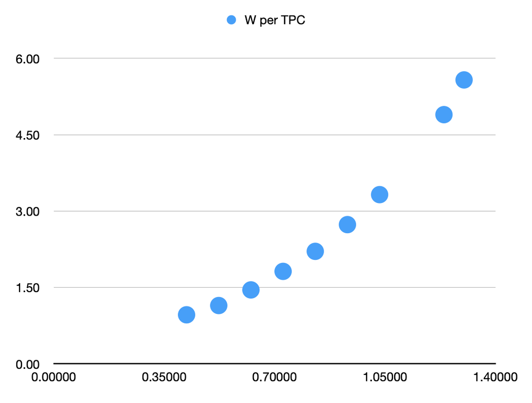
We can see that the power consumption curves upwards as clock speeds increase. The reason for this is that to increase clock speed you need to increase voltage, and power consumption is proportional to voltage squared. As a result, higher clock speeds are typically less efficient than lower ones.
So, if higher clock speeds are typically less efficient, doesn't that mean you can always reduce clocks to gain efficiency? Not quite. While the chart above might look like a smooth curve, it's actually hiding something; at that lowest clock speed of 420MHz the curve breaks down completely. To illustrate, let's look at the same data, but chart power efficiency (measured in Gflops per Watt) rather than outright power consumption:
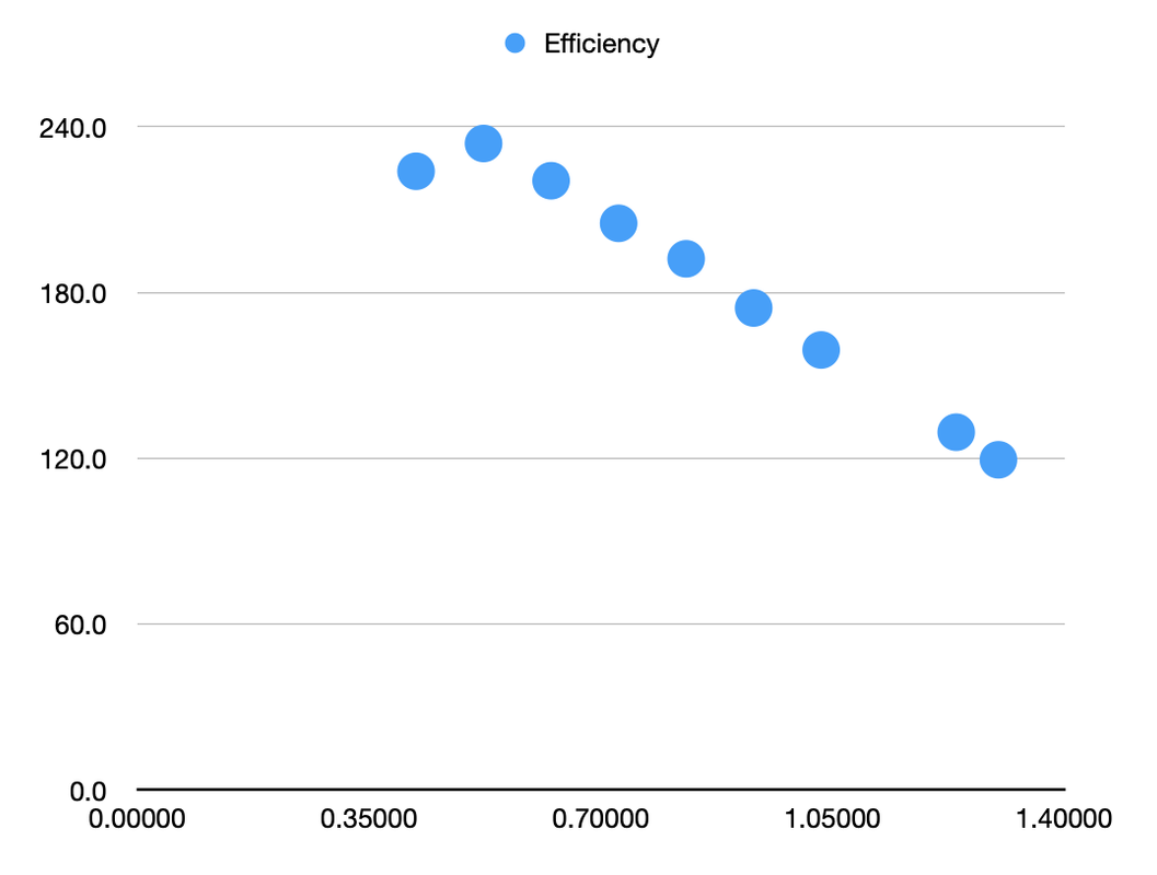
There are two things going on in this chart. For all the data points from 522 MHz onwards, we see what you would usually expect, which is that efficiency drops as clock speeds increase. The relationship is exceptionally clear here, as it's a pretty much perfect straight line. But then there's that point on the left. The GPU at 420MHz is less efficient than it is at 522MHz, why is that?
The answer is relatively straight-forward if we consider one important point: there is a minimum voltage that the chip can operate at. Voltage going up with clock speed means efficiency gets worse, and voltage going down as clock speeds increase means efficiency gets better. But what happens when you want to reduce clocks but can't reduce voltage any more? Not only do you stop improving power efficiency, but it actually starts to go pretty sharply in the opposite direction.
Because power consumption is mostly related to voltage, not clock speed, when you reduce clocks but keep the voltage the same, you don't really save much power. A large part of the power consumption called "static power" stays exactly the same, while the other part, "dynamic power", does fall off a bit. What you end up with is much less performance, but only slightly less power consumption. That is, power efficiency gets worse.
So that kink in the efficiency graph, between 420MHz and 522MHz, is the point at which you can't reduce the voltage any more. Any clocks below that point will all operate at the same voltage, and without being able to reduce the voltage, power efficiency gets worse instead of better below that point. The clock speed at that point can be called the "peak efficiency clock", as it offers higher power efficiency than any other clock speed.
How does this impact how chips are designed?
There are two things to take from the above. First, as a general point, every chip on a given manufacturing process has a peak efficiency clock, below which you lose power efficiency by reducing clocks. Secondly, we have the data from Orin to know pretty well where this point is for a GPU very similar to T239's on a Samsung 8nm process, which is around 470MHz.
Now let's talk designing chips. Nvidia and Nintendo are in a room deciding what GPU to put in their new SoC for Nintendo's new console. Nintendo has a financial budget of how much they want to spend on the chip, but they also have a power budget, which is how much power the chip can use up to keep battery life and cooling in check. Nvidia and Nintendo's job in that room is to figure out the best GPU they can fit within those two budgets.
GPUs are convenient in that you can make them basically as wide as you want (that is use as many SMs as you want) and developers will be able to make use of all the performance available. The design space is basically a line between a high number of SMs at a low clock, and a low number of SMs at a high clock. Because there's a fixed power budget, the theoretically ideal place on that line is the one where the clock is the peak efficiency clock, so you can get the most performance from that power.
That is, if the power budget is 3W for the GPU, and the peak efficiency clock is 470MHz, and the power consumption per SM at 470MHz is 0.5W, then the best possible GPU they could include would be a 6 SM GPU running at 470MHz. Using a smaller GPU would mean higher clocks, and efficiency would drop, but using a larger GPU with lower clocks would also mean efficiency would drop, because we're already at the peak efficiency clock.
In reality, it's rare to see a chip designed to run at exactly that peak efficiency clock, because there's always a financial budget as well as the power budget. Running a smaller GPU at higher clocks means you save money, so the design is going to be a tradeoff between a desire to get as close as possible to the peak efficiency clock, which maximises performance within a fixed power budget, and as small a GPU as possible, which minimises cost. Taking the same example, another option would be to use 4 SMs and clock them at around 640MHz. This would also consume 3W, but would provide around 10% less performance. It would, however, result in a cheaper chip, and many people would view 10% performance as a worthwhile trade-off when reducing the number of SMs by 33%.
However, while it's reasonable to design a chip with intent to clock it at the peak efficiency clock, or to clock it above the peak efficiency clock, what you're not going to see is a chip that's intentionally designed to run at a fixed clock speed that's below the peak efficiency clock. The reason for this is pretty straight-forward; if you have a design with a large number of SMs that's intended to run at a clock below the peak efficiency clock, you could just remove some SMs and increase the clock speed and you would get both better performance within your power budget and it would cost less.
How does this relate to Nintendo and T239's manufacturing process?
The above section wasn't theoretical. Nvidia and Nintendo did sit in a room (or have a series of calls) to design a chip for a new Nintendo console, and what they came out with is T239. We know that the result of those discussions was to use a 12 SM Ampere GPU. We also know the power curve, and peak efficiency clock for a very similar Ampere GPU on 8nm.
The GPU in the TX1 used in the original Switch units consumed around 3W in portable mode, as far as I can tell. In later models with the die-shrunk Mariko chip, it would have been lower still. Therefore, I would expect 3W to be a reasonable upper limit to the power budget Nintendo would allocate for the GPU in portable mode when designing the T239.
With a 3W power budget and a peak efficiency clock of 470MHz, then the (again, not theoretical) numbers above tell us the best possible performance would be achieved by a 6 SM GPU operating at 470MHz, and that you'd be able to get 90% of that performance with a 4 SM GPU operating at 640MHz. Note that neither of these say 12 SMs. A 12 SM GPU on Samsung 8nm would be an awful design for a 3W power budget. It would be twice the size and cost of a 6 SM GPU while offering much less performance, if it's even possible to run within 3W at any clock.
There's no world where Nintendo and Nvidia went into that room with an 8nm SoC in mind and a 3W power budget for the GPU in handheld mode, and came out with a 12 SM GPU. That means either the manufacturing process, or the power consumption must be wrong (or both). I'm basing my power consumption estimates on the assumption that this is a device around the same size as the Switch and with battery life that falls somewhere between TX1 and Mariko units. This seems to be the same assumption almost everyone here is making, and while it could be wrong, I think them sticking with the Switch form-factor and battery life is a pretty safe bet, which leaves the manufacturing process.
So, if it's not Samsung 8nm, what is it?
Well, from the Orin data we know that a 12 SM Ampere GPU on Samsung 8nm at the peak efficiency clocks of 470MHz would consume a bit over 6W, which means we need something twice as power efficient as Samsung 8nm. There are a couple of small differences between T239 and Orin's GPUs, like smaller tensor cores and improved clock-gating, but they are likely to have only marginal impact on power consumption, nowhere near the 2x we need, which will have to come from a better manufacturing process.
One note to add here is that we actually need a bit more than a 2x efficiency improvement over 8nm, because as the manufacturing process changes, so does the peak efficiency clock. The peak efficiency clock will typically increase as an architecture is moved to a more efficient manufacturing process, as the improved process allows higher clocks at given voltages. From DVFS tables in Linux, we know that Mariko's peak efficiency clock on 16nm/12nm is likely 384MHz. That's increased to around 470MHz for Ampere on 8nm, and will increase further as it's migrated to more advanced processes.
I'd expect peak efficiency clocks of around 500-600MHz on improved processes, which means that instead of running at 470MHz the chip would need to run at 500-600MHz within 3W to make sense. A clock of 550MHz would consume around 7.5W on 8nm, so we would need a 2.5x improvement in efficiency instead.
So, what manufacturing process can give a 2.5x improvement in efficiency over Samsung 8nm? The only reasonable answer I can think of is TSMC's 5nm/4nm processes, including 4N, which just happens to be the process Nvidia is using for every other product (outside of acquired Mellanox products) from this point onwards. In Nvidia's Ada white paper (an architecture very similar to Ampere), they claim a 2x improvement in performance per Watt, which appears to come almost exclusively from the move to TSMC's 4N process, plus some memory changes.
They don't provide any hard numbers for similarly sized GPUs at the same clock speed, with only a vague unlabelled marketing graph here, but they recently announced the Ada based RTX 4000 SFF workstation GPU, which has 48 SMs clocked at 1,565MHz and a 70W TDP. The older Ampere RTX A4000 also had 48 SMs clocked at 1,560MHz and had a TDP of 140W. There are differences in the memory setup, and TDPs don't necessarily reflect real world power consumption, but the indication is that the move from Ampere on Samsung 8nm to an Ampere-derived architecture on TSMC 4N reduces power consumption by about a factor of 2.
What about the other options? TSMC 6nm or Samsung 5nm/4nm?
Honestly the more I think about it the less I think these other possibilities are viable. Even aside from the issue that these aren't processes Nvidia is using for anything else, I just don't think a 12 SM GPU would make sense on either of them. Even on TSMC 4N it's a stretch. Evidence suggests that it would achieve a 2x efficiency improvement, but we would be looking for 2.5x in reality. There's enough wiggle room there, in terms of Ada having some additional features not in T239 and not having hard data on Ada's power consumption, so the actual improvement in T239's case may be 2.5x, but even that would mean that Nintendo have gone for the largest GPU possible within the power limit.
With 4N just about stretching to the 2.5x improvement in efficiency required for a 12 SM GPU to make sense, I don't think the chances for any other process are good. We don't have direct examples for other processes like we have for Ada, but from everything we know, TSMC's 5nm class processes are significantly more efficient than either their 6nm or Samsung's 5nm/4nm processes. If it's a squeeze for 12 SMs to work on 4N, then I can't see how it would make sense on anything less efficient than 4N.
But what about cost, isn't 4nm really expensive?
Actually, no. TSMC's 4N wafers are expensive, but they're also much higher density, which means you fit many more chips on a wafer. This SemiAnalysis article from September claimed that Nvidia pays 2.2x as much for a TSMC 4N wafer as they do for a Samsung 8nm wafer. However, Nvidia is achieving 2.7x higher transistor density on 4N, which means that a chip with the same transistor count would actually be cheaper if manufactured on 4N than 8nm (even more so when you factor yields into account).
Are there any caveats?
Yes, the major one being the power consumption of the chip. I'm assuming that Nintendo's next device is going to be roughly the same size and form-factor as the Switch, and they will want a similar battery life. If it's a much larger device (like Steam Deck sized) or they're ok with half an hour of battery life, then that changes the equations, but I don't think either of those are realistic. Ditto if it turned out to be a stationary home console for some reason (again, I'm not expecting that).
The other one is that I'm assuming that Nintendo will use all 12 SMs in portable mode. It's theoretically possible that they would disable half of them in portable mode, and only run the full 12 in docked mode. This would allow them to stick within 3W even on 8nm. However, it's a pain from the software point of view, and it assumes that Nintendo is much more focussed on docked performance than handheld, including likely running much higher power draw docked. I feel it's more likely that Nintendo would build around handheld first, as that's the baseline of performance all games will have to operate on, and then use the same setup at higher clocks for docked.
That's a lot of words. Is this just all confirmation bias or copium or hopium or whatever the kids call it?
I don't think so. Obviously everyone should be careful of their biases, but I actually made the exact same argument over a year ago back before the Nvidia hack, when we thought T239 would be manufactured on Samsung 8nm but didn't know how big the GPU was. At the time a lot of people thought I was too pessimistic because I thought 8 SMs was unrealistic on 8nm and a 4 SM GPU was more likely. I was wrong about T239 using a 4 SM GPU, but the Orin power figures we got later backed up my argument, and 8 SMs is indeed unrealistic on 8nm. The 12 SM GPU we got is even more unrealistic on 8nm, so by the same logic we must be looking at a much more efficient manufacturing process. What looked pessimistic back then is optimistic now only because the data has changed.
That's assuming they went with A72 and 16nm... Which would be a bit much. And I don't think they would've clocked it high enough to hit double CPU performance versus OG Switch, especially as CPU clocks needed to be maintained between Portable and docked modeThe cpu could have been close to twice as powerful. Which would have really helped porting from other consoles.
backward compatibly is much more important then a fancy display, you can live with a inferior display technology, but not with backward compatibly, if i was Nintendo i would priorize backward compatiblePeople can want both backwards compatibility and an OLED screen. I don't know about as a whole, but between the Switch LCD and Switch OLED screens... I'd take the OLED any day, it's felt like a night and day difference since I upgraded. I'd feel really disappointed if the Switch successor had an LCD screen unless it's a significant step up over the current Switch's.
I asked before and @oldpuck explained that too big a gap in performance between docked and undocked would create a Series S/X problem of devs having to effectively make two different versions of games.I haven't seen the reasoning as to why they couldn't let the docked Switch 2 use more electricity than the docked Switch 1.
To be fair, a Switch Targeting 4K output in general would be in that situation to some extent anyway due to the sheer difference of power needed for 720p output versus 4K (even if upscaled via DLSS) output.I asked before and @oldpuck explained that too big a gap in performance between docked and undocked would create a Series S/X problem of devs having to effectively make two different versions of games.

I don't understand what your point is, I guess. I haven't seen anyone say that they want OLED more than backwards compatibility. I don't really understand why you're comparing the two.backward compatibly is much more important then a fancy display, you can live with a inferior display technology, but not with backward compatibly, if i was Nintendo i would priorize backward compatible
This is a nothing article for us famifriends. Nothing new here for us. Apart from Dev kits which we know about, the rest is speculation.
Edit: omg there are 7 new pages since this quoted post...
This is a nothing article for us famifriends. Nothing new here for us. Apart from Dev kits which we know about, the rest is speculation.
Edit: omg there are 7 new pages since this quoted post...
There's a lot of things in this. First is the fact that there's confirmation from multiple sources that devkits are on the Wild. Second is, due to the fact VGC sources are on the western side, Switch 2 devkits are being rolled out to more partners worldwide. And the third one is the fact there's another source reaffirming Nikkei timeframe for the console launch (late 24). To not mention the LCD screen possibility, higher storage amount, etc.This is a nothing article for us famifriends. Nothing new here for us. Apart from Dev kits which we know about, the rest is speculation.
Edit: omg there are 7 new pages since this quoted post...
People can want both backwards compatibility and an OLED screen. I don't know about as a whole, but between the Switch LCD and Switch OLED screens... I'd take the OLED any day, it's felt like a night and day difference since I upgraded. I'd feel really disappointed if the Switch successor had an LCD screen unless it's a significant step up over the current Switch's.
Being a VR nerd, I do happen to be aware of at least a couple devices that use very small miniLED displays (the Varjo Aero in October 2021 and the Meta Quest Pro in October 2022). Here is a comparison between OLED and miniLED tech with local dimming - shout out to SadlyItsBradley on Twitter. Needless to say, miniLED displays in an even smaller form factor than the current Switch have already been mass produced for multiple products.
The difference between a standard LCD display with an LED backlight from the last decade and an LCD with miniLED local dimming is actually pretty stark, so I wouldn't be too worried about the fact that the Sharp report mentions LCD. While minLED doesn't have per-pixel backlight control like OLED, it can actually get a lot brighter than OLED without burn-in issues due to being inorganic tech (vs the organic "O" in "OLED" that makes them much more susceptible to degradation over time) which can have ramifications for possible HDR capabilities.
It's absolutely a downgrade for the millions of current Switch OLED owners.LCD is not a downgrade, OLED is much more expensive and risk your display of burn-in, i would be extremely/more worried for lact of backward compatibility then OLED display on Nintendo next gen hardware, dont you all realize OLED was only meant for the Switch Pro that became Switch OLED.
Thanks for the insight! If it is actually miniLED, I'd certainly feel a lot more optimistic. I'm not exactly feeling pessimistic, I guess, but the idea of going from OLED to an LCD screen like the base Switch's is... not appealing lol.With all this discussion around LCD vs OLED, I feel this discussion surrounding the SHARP manufacturing rumors is once again relevant (emphasis added):
TL;DR - LCD as mentioned in the VGC article can very possibly be referring to miniLED, which can (and already does in some instances) surpass OLED in quality in several metrics.
We already know about the Spanish devkits. So maybe VGC are just using that as their "source". Or maybe another studio they know did receive one as well but we already know about the Spanish one/s.Why exactly? Cause we had one source saying one studio in Italy or something got one? That's all you needed and you were good?
This is not confirmed yet.Nothing new? We’ve had a large % of posters thinking it was coming this year with some even expecting a reveal this month.
miniLED surpasses OLED in total brightness, and that's pretty much it. Contrast ratio, black levels, viewing angles, etc, are all superior on OLED.With all this discussion around LCD vs OLED, I feel this discussion surrounding the SHARP manufacturing rumors is once again relevant (emphasis added):
TL;DR - LCD as mentioned in the VGC article can very possibly be referring to miniLED, which can (and already does in some instances) surpass OLED in quality in several metrics.
While i agree we sort of guessed a lot of these, this is confirmation of specific details that we can later check to see if it's BS or not.This is a nothing article for us famifriends. Nothing new here for us. Apart from Dev kits which we know about, the rest is speculation.
Edit: omg there are 7 new pages since this quoted post...
DSiWare ran the same as DS cartridge games on 3DS, using a hardware-based DSi-mode.
miniLED surpasses OLED in total brightness, and that's pretty much it. Contrast ratio, black levels, viewing angles, etc, are all superior on OLED.
One of the reasons manufacturers opt for miniLED backlighting is because they can create smaller, more precise dimming zones to try and reduce blooming. Using a miniLED backlight, developing local dimming algorithms, and then implementing a dedicated chip to control the backlight quickly enough for gaming would all be more expensive than just using an OLED panel.
If Nintendo is trying to cut corners and save costs by going with the cheaper LCD display, it's going to have a regular LED backlight with no local dimming.
Assuming Sharp's indeed providing LCD displays for Nintendo's next-gen console, then potentially support for VRR at ≥720p. Mobile OLED displays, as far as I know, only support VRR at ≥1080p.
LCD is not a downgrade, OLED is much more expensive and risk your display of burn-in, i would be extremely/more worried for lact of backward compatibility then OLED display on Nintendo next gen hardware, dont you all realize OLED was only meant for the Switch Pro that became Switch OLED.
We really wrestled with the node question, and i think most of us were team 8nm for a long time.Thank you!
Why does almost everyone here expects that Nvidia and Nintendo will use TSMC 4N (instead of Samsung 8nm process, the ‘default’ one for T234 Orin) ?
I haven't seen the reasoning as to why they couldn't let the docked Switch 2 use more electricity than the docked Switch 1.
I mean, it can use more electricity! But the gap probably can't be much larger, because yeah, the performance gap starts to get bad. 2x perf was where the Switch originally targeted, and they made that smaller. 3x is the Series S/X gap, and devs complain it's too big to manage. By 4x it's a full generation in difference.I asked before and @oldpuck explained that too big a gap in performance between docked and undocked would create a Series S/X problem of devs having to effectively make two different versions of games.