My guess is currently 1.7 Tflops in portable mode (12 SMs @ 550MHz) and 3.4 Tflops docked (12 SMs @ 1.1GHz).
To explain my reasoning, let's play a game of
Why does Thraktor think a TSMC 4N manufacturing process is likely for T239?
The short answer is that a 12 SM GPU is far too large for Samsung 8nm, and likely too large for any intermediate process like TSMC's 6nm or Samsung's 5nm/4nm processes. There's a popular conception that Nintendo will go with a "cheap" process like 8nm and clock down to oblivion in portable mode, but that ignores both the economic and physical realities of microprocessor design.
To start, let's quickly talk about
power curves. A power curve for a chip, whether a CPU or GPU or something else, is a plot of the amount of power the chip consumes against the clock speed of the chip. A while ago I extracted the power curve for Orin's 8nm Ampere GPU from a Nvidia power estimator tool. There are more in-depth details
here,
here and
here, but for now let's focus on the actual power curve data:
Code:
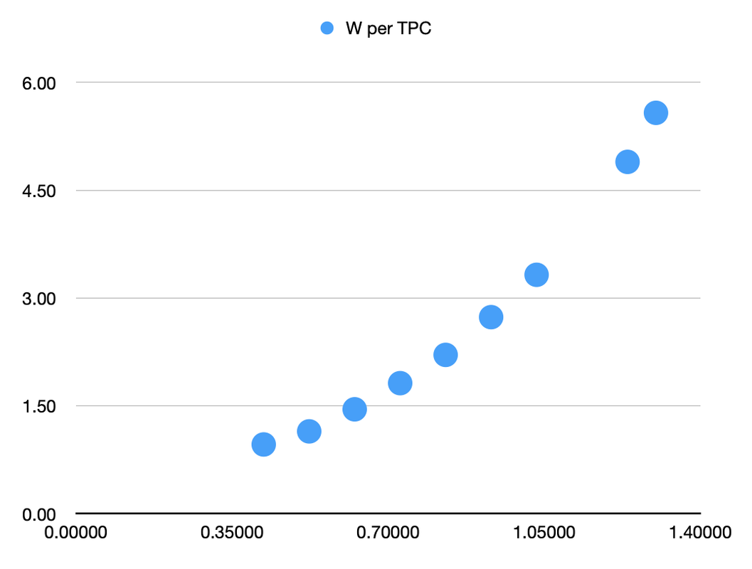
Clock      W per TPC
0.42075    0.96
0.52275    1.14
0.62475    1.45
0.72675    1.82
0.82875    2.21
0.93075    2.73
1.03275    3.32
1.23675    4.89
1.30050    5.58
The first column is the clock speed in GHz, and the second is the Watts consumed per TPC (which is a pair of SMs). Let's create a chart for this power curve:
We can see that the power consumption curves upwards as clock speeds increase. The reason for this is that to increase clock speed you need to increase voltage, and power consumption is proportional to voltage squared. As a result, higher clock speeds are typically less efficient than lower ones.
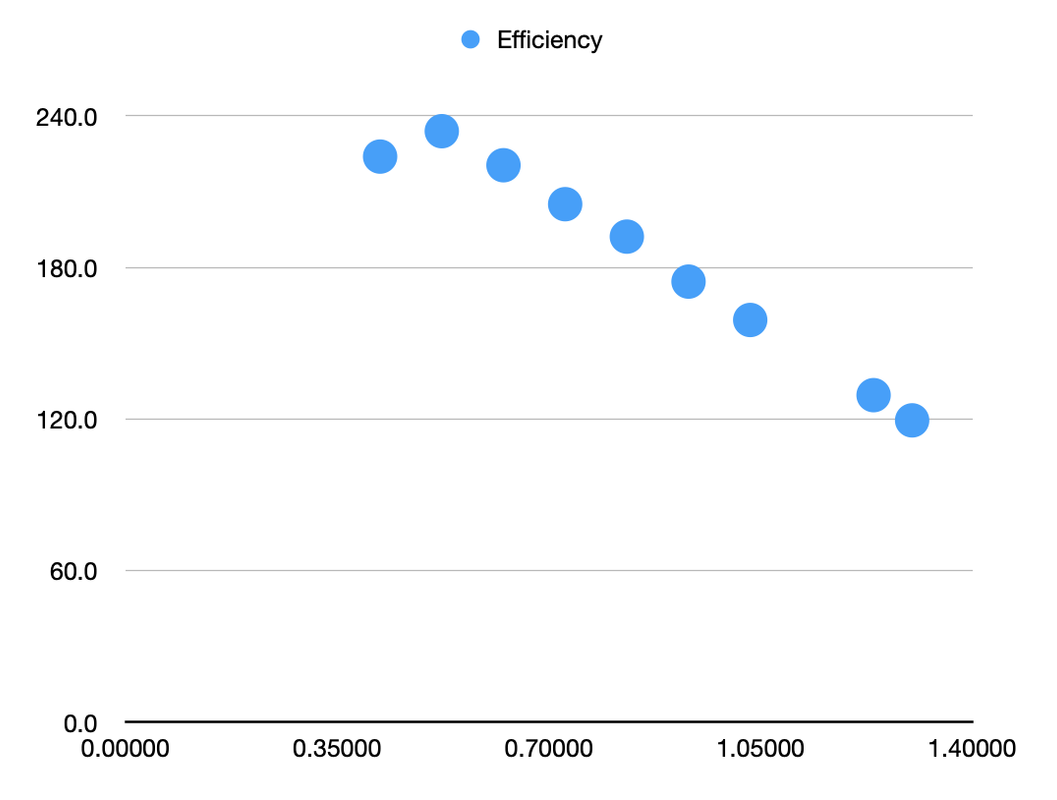
So, if higher clock speeds are typically less efficient, doesn't that mean you can always reduce clocks to gain efficiency? Not quite. While the chart above might look like a smooth curve, it's actually hiding something; at that lowest clock speed of 420MHz the curve breaks down completely. To illustrate, let's look at the same data, but chart power efficiency (measured in Gflops per Watt) rather than outright power consumption:
There are two things going on in this chart. For all the data points from 522 MHz onwards, we see what you would usually expect, which is that efficiency drops as clock speeds increase. The relationship is exceptionally clear here, as it's a pretty much perfect straight line. But then there's that point on the left. The GPU at 420MHz is
less efficient than it is at 522MHz, why is that?
The answer is relatively straight-forward if we consider one important point:
there is a minimum voltage that the chip can operate at. Voltage going up with clock speed means efficiency gets worse, and voltage going down as clock speeds increase means efficiency gets better. But what happens when you want to reduce clocks but can't reduce voltage any more? Not only do you stop improving power efficiency, but it actually starts to go pretty sharply in the opposite direction.
Because power consumption is mostly related to voltage, not clock speed, when you reduce clocks but keep the voltage the same, you don't really save much power. A large part of the power consumption called "static power" stays exactly the same, while the other part, "dynamic power", does fall off a bit. What you end up with is much less performance, but only slightly less power consumption. That is, power efficiency gets worse.
So that kink in the efficiency graph, between 420MHz and 522MHz, is the point at which you can't reduce the voltage any more. Any clocks below that point will all operate at the same voltage, and without being able to reduce the voltage, power efficiency gets worse instead of better below that point. The clock speed at that point can be called the "peak efficiency clock", as it offers higher power efficiency than any other clock speed.
How does this impact how chips are designed?
There are two things to take from the above. First, as a general point, every chip on a given manufacturing process has a peak efficiency clock, below which you
lose power efficiency by reducing clocks. Secondly, we have the data from Orin to know pretty well where this point is for a GPU very similar to T239's on a Samsung 8nm process, which is around 470MHz.
Now let's talk designing chips. Nvidia and Nintendo are in a room deciding what GPU to put in their new SoC for Nintendo's new console. Nintendo has a financial budget of how much they want to spend on the chip, but they also have a
power budget, which is how much power the chip can use up to keep battery life and cooling in check. Nvidia and Nintendo's job in that room is to figure out the best GPU they can fit within those two budgets.
GPUs are convenient in that you can make them basically as wide as you want (that is use as many SMs as you want) and developers will be able to make use of all the performance available. The design space is basically a line between a high number of SMs at a low clock, and a low number of SMs at a high clock. Because there's a fixed power budget, the theoretically ideal place on that line is the one where the clock is the peak efficiency clock, so you can get the most performance from that power.
That is, if the power budget is 3W for the GPU, and the peak efficiency clock is 470MHz, and the power consumption per SM at 470MHz is 0.5W, then the best possible GPU they could include would be a 6 SM GPU running at 470MHz. Using a smaller GPU would mean higher clocks, and efficiency would drop, but using a larger GPU with lower clocks would
also mean efficiency would drop, because we're already at the peak efficiency clock.
In reality, it's rare to see a chip designed to run at exactly that peak efficiency clock, because there's always a financial budget as well as the power budget. Running a smaller GPU at higher clocks means you save money, so the design is going to be a tradeoff between a desire to get as close as possible to the peak efficiency clock, which maximises performance within a fixed power budget, and as small a GPU as possible, which minimises cost. Taking the same example, another option would be to use 4 SMs and clock them at around 640MHz. This would also consume 3W, but would provide around 10% less performance. It would, however, result in a cheaper chip, and many people would view 10% performance as a worthwhile trade-off when reducing the number of SMs by 33%.
However, while it's reasonable to design a chip with intent to clock it at the peak efficiency clock, or to clock it above the peak efficiency clock, what you're
not going to see is a chip that's intentionally designed to run at a fixed clock speed that's
below the peak efficiency clock. The reason for this is pretty straight-forward; if you have a design with a large number of SMs that's intended to run at a clock below the peak efficiency clock, you could just remove some SMs and increase the clock speed and you would get both better performance within your power budget
and it would cost less.
How does this relate to Nintendo and T239's manufacturing process?
The above section wasn't theoretical. Nvidia and Nintendo did sit in a room (or have a series of calls) to design a chip for a new Nintendo console, and what they came out with is T239. We know that the result of those discussions was to use a 12 SM Ampere GPU. We also know the power curve, and peak efficiency clock for a very similar Ampere GPU on 8nm.
The GPU in the TX1 used in the original Switch units consumed around 3W in portable mode, as far as I can tell. In later models with the die-shrunk Mariko chip, it would have been lower still. Therefore, I would expect 3W to be a reasonable upper limit to the power budget Nintendo would allocate for the GPU in portable mode when designing the T239.
With a 3W power budget and a peak efficiency clock of 470MHz, then the (again, not theoretical) numbers above tell us the best possible performance would be achieved by a 6 SM GPU operating at 470MHz, and that you'd be able to get 90% of that performance with a 4 SM GPU operating at 640MHz. Note that neither of these say 12 SMs. A 12 SM GPU on Samsung 8nm would be an awful design for a 3W power budget. It would be twice the size and cost of a 6 SM GPU while offering much less performance, if it's even possible to run within 3W at any clock.
There's no world where Nintendo and Nvidia went into that room with an 8nm SoC in mind and a 3W power budget for the GPU in handheld mode, and came out with a 12 SM GPU. That means either the manufacturing process, or the power consumption must be wrong (or both). I'm basing my power consumption estimates on the assumption that this is a device around the same size as the Switch and with battery life that falls somewhere between TX1 and Mariko units. This seems to be the same assumption almost everyone here is making, and while it could be wrong, I think them sticking with the Switch form-factor and battery life is a pretty safe bet, which leaves the manufacturing process.
So, if it's not Samsung 8nm, what is it?
Well, from the Orin data we know that a 12 SM Ampere GPU on Samsung 8nm at the peak efficiency clocks of 470MHz would consume a bit over 6W, which means we need something twice as power efficient as Samsung 8nm. There are a couple of small differences between T239 and Orin's GPUs, like smaller tensor cores and improved clock-gating, but they are likely to have only marginal impact on power consumption, nowhere near the 2x we need, which will have to come from a better manufacturing process.
One note to add here is that we actually need a bit more than a 2x efficiency improvement over 8nm, because as the manufacturing process changes, so does the peak efficiency clock. The peak efficiency clock will typically increase as an architecture is moved to a more efficient manufacturing process, as the improved process allows higher clocks at given voltages. From DVFS tables in Linux, we know that Mariko's peak efficiency clock on 16nm/12nm is likely 384MHz. That's increased to around 470MHz for Ampere on 8nm, and will increase further as it's migrated to more advanced processes.
I'd expect peak efficiency clocks of around 500-600MHz on improved processes, which means that instead of running at 470MHz the chip would need to run at 500-600MHz within 3W to make sense. A clock of 550MHz would consume around 7.5W on 8nm, so we would need a 2.5x improvement in efficiency instead.
So, what manufacturing process can give a 2.5x improvement in efficiency over Samsung 8nm? The only reasonable answer I can think of is TSMC's 5nm/4nm processes, including 4N, which just happens to be the process Nvidia is using for every other product (outside of acquired Mellanox products) from this point onwards. In
Nvidia's Ada white paper (an architecture very similar to Ampere), they claim a 2x improvement in performance per Watt, which appears to come almost exclusively from the move to TSMC's 4N process, plus some memory changes.
They don't provide any hard numbers for similarly sized GPUs at the same clock speed, with only a vague unlabelled marketing graph
here, but they recently announced the Ada based
RTX 4000 SFF workstation GPU, which has 48 SMs clocked at 1,565MHz and a 70W TDP. The older Ampere
RTX A4000 also had 48 SMs clocked at 1,560MHz and had a TDP of 140W. There are differences in the memory setup, and TDPs don't necessarily reflect real world power consumption, but the indication is that the move from Ampere on Samsung 8nm to an Ampere-derived architecture on TSMC 4N reduces power consumption by about a factor of 2.
What about the other options? TSMC 6nm or Samsung 5nm/4nm?
Honestly the more I think about it the less I think these other possibilities are viable. Even aside from the issue that these aren't processes Nvidia is using for anything else, I just don't think a 12 SM GPU would make sense on either of them. Even on TSMC 4N it's a stretch. Evidence suggests that it would achieve a 2x efficiency improvement, but we would be looking for 2.5x in reality. There's enough wiggle room there, in terms of Ada having some additional features not in T239 and not having hard data on Ada's power consumption, so the actual improvement in T239's case may be 2.5x, but even that would mean that Nintendo have gone for the largest GPU possible within the power limit.
With 4N just about stretching to the 2.5x improvement in efficiency required for a 12 SM GPU to make sense, I don't think the chances for any other process are good. We don't have direct examples for other processes like we have for Ada, but from everything we know, TSMC's 5nm class processes are significantly more efficient than either their 6nm or Samsung's 5nm/4nm processes. If it's a squeeze for 12 SMs to work on 4N, then I can't see how it would make sense on anything less efficient than 4N.
But what about cost, isn't 4nm really expensive?
Actually, no. TSMC's 4N wafers are expensive, but they're also much higher density, which means you fit many more chips on a wafer.
This SemiAnalysis article from September claimed that Nvidia pays 2.2x as much for a TSMC 4N wafer as they do for a Samsung 8nm wafer. However, Nvidia is achieving 2.7x higher transistor density on 4N, which means that a chip with the same transistor count would actually be cheaper if manufactured on 4N than 8nm (even more so when you factor yields into account).
Are there any caveats?
Yes, the major one being the power consumption of the chip. I'm assuming that Nintendo's next device is going to be roughly the same size and form-factor as the Switch, and they will want a similar battery life. If it's a much larger device (like Steam Deck sized) or they're ok with half an hour of battery life, then that changes the equations, but I don't think either of those are realistic. Ditto if it turned out to be a stationary home console for some reason (again, I'm not expecting that).
The other one is that I'm assuming that Nintendo will use all 12 SMs in portable mode. It's theoretically possible that they would disable half of them in portable mode, and only run the full 12 in docked mode. This would allow them to stick within 3W even on 8nm. However, it's a pain from the software point of view, and it assumes that Nintendo is much more focussed on docked performance than handheld, including likely running much higher power draw docked. I feel it's more likely that Nintendo would build around handheld first, as that's the baseline of performance all games will have to operate on, and then use the same setup at higher clocks for docked.
That's a lot of words. Is this just all confirmation bias or copium or hopium or whatever the kids call it?
I don't think so. Obviously everyone should be careful of their biases, but I actually made the exact same argument
over a year ago back before the Nvidia hack, when we thought T239 would be manufactured on Samsung 8nm but didn't know how big the GPU was. At the time a lot of people thought I was too pessimistic because I thought 8 SMs was unrealistic on 8nm and a 4 SM GPU was more likely. I was wrong about T239 using a 4 SM GPU, but the Orin power figures we got later backed up my argument, and 8 SMs is indeed unrealistic on 8nm. The 12 SM GPU we got is even more unrealistic on 8nm, so by the same logic we must be looking at a much more efficient manufacturing process. What looked pessimistic back then is optimistic now only because the data has changed.

, a [redacted] exclusive, at launch, with maybe a couple of other exclusives over the year, and the rest of the lineup consisting of cross-gen games. Let's also say that Major Flagship Game

")