I'd caution from reading
too much into comparisons with SSDs. Although the underlying technology is similar (we think), the implementation is very different. In particular, SSDs achieve high read speeds via parallelisation across several NAND chips. Game cards only use a single chip, so we should expect speeds to be lower, perhaps substantially so. There are also potentially other limitations like power consumption or the performance of the security ASIC which may limit things further.
As per
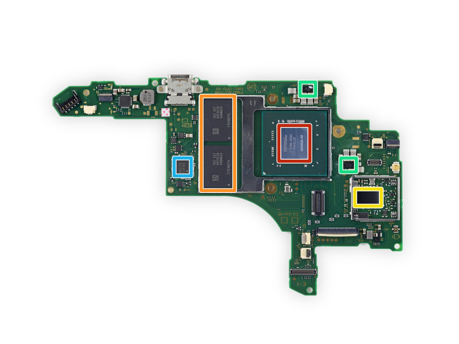
SwitchBrew, the game card uses an 8 bit SPI-style interface. Supported clock speeds are
25MHz and 50MHz, which gives bandwidth of either 25MB/s or 50MB/s.
If [redacted] to use the same game card format without extra pins, then the limit (aside from the game cards themselves, security ASICs, etc.) would be how high they can clock the interface. Unfortunately I can't find many examples of SPI-style interfaces clocking significantly higher than this. Most SPI devices max out at around 50MHz or so, with a couple at about 100MHz. I don't think this represents a limit of the technology, as you can easily find 20 year old devices using 50MHz SPI interfaces, it's just that manufacturers have moved away from SPI to other interfaces when they need hundreds of MB/s.
I'd be surprised if they went with a substantially higher SPI interface speed, though (ie more than 100-200MHz). Both
DS and 3DS game cards also used an 8 bit SPI-style interface (different from Switch's, though), with the DS using 4.2MHz/6.7MHz clocks, and the 3DS using 16.6MHz. That means that over the past three generations of game cards, they've increased the interface speed by about 3x each time. Continuing on the same trend, we'd expect a clock of around 150MHz, and read speeds of around 150MB/s on [redacted] game cards if they update the existing interface.
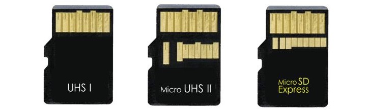
The alternative would be to use a different interface than SPI. If they want to maintain backwards compatibility, that would mean adding extra pins, as with the SD examples. There are, of course, a lot of options available to them. One lane (4 data pins) of PCIe 4.0 would give them up to 2GB/s of bandwidth. MIPI M-PHY 4.1 with two lanes (4 data pins) would exceed 2GB/s, and one lane (2 data pins) would exceed 1GB/s. Both of these interfaces are built into Orin already, and presumably T239, too. These are overkill for Nintendo's use-case, though, as they're both bi-directional, whereas Nintendo only needs high speeds in one direction. MIPI's D-PHY is perhaps more suitable as an out-of-the-box option for asymmetrical data requirements, which is commonly used for cameras and displays in mobile devices. The latest spec would achieve speeds of about 1GB/s. Nintendo could also design their own interface, as they have done up to this point.
One potential issue with adding extra pins is where you place them. The pins on the Switch game card already take up almost half of the back of the card. Adding another row above it wouldn't really leave much space to hold it. Perhaps they could make the card a bit wider and add another column of pins for the new protocol, although they'd have to do so in a way that it's easy and obvious how to insert existing Switch game cards into the same slot.