• Hey everyone, staff have documented a list of banned content and subject matter that we feel are not consistent with site values, and don't make sense to host discussion of on Famiboards. This list (and the relevant reasoning per item) is viewable here.
  • Do you have audio editing experience and want to help out with the Famiboards Discussion Club Podcast? If so, we're looking for help and would love to have you on the team! Just let us know in the Podcast Thread if you are interested!

StarTopic Future Nintendo Hardware & Technology Speculation & Discussion |ST| (Read the staff posts before commenting!)

Same for me. But device size can’t grow forever…


…or can it?
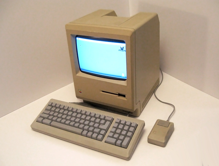
behold, the switch 5 form factor (it has a handle!)

macintosh128.jpg
 
8nm started with Tegra Orin, which is 8N

Kopite7Kimi admits to not knowing and assumed 8N based on Orin

For all intents and purposes, 4N is a 5nm design

We just don't know. The discussion centers around 8nm vs 4N, but realistically it could just as easily be Samsung 5nm. Rumors from long ago suggested that a deal was struck with Samsung to supply multiple components for Nintendos next hardware. Taking on a very low margin/break even SOC deal might be off the table for Samsung if it were by itself, but by bundling in internal memory, game card Nand and maybe the LCD screen, now that is something that could make sense. So I would say Samsung 5nm is just as likely as TSMC 4N, and just because it's performance is not as good as 4N doesn't mean much for this product.
 
We just don't know. The discussion centers around 8nm vs 4N, but realistically it could just as easily be Samsung 5nm. Rumors from long ago suggested that a deal was struck with Samsung to supply multiple components for Nintendos next hardware. Taking on a very low margin/break even SOC deal might be off the table for Samsung if it were by itself, but by bundling in internal memory, game card Nand and maybe the LCD screen, now that is something that could make sense. So I would say Samsung 5nm is just as likely as TSMC 4N, and just because it's performance is not as good as 4N doesn't mean much for this product.
I think the problem with this is that the T239 SoC is a nvidia product, plus nvidia products (in the present time frame) are predominantly either Samsung 8N or TSMC 4N. Has there been nvidia products based on Samsung 5nm?

I don't know much about lithography in general, but my impression is that it's not the kind of thing where nvidia could just assign one of their chips to a random foundry, when they already have processes in place working with SEC8N or TSMC 4N. As a matter of fact, TSMC 4N is a node process customized specifically for nvidia, no other TSMC customers uses TSMC 4N.
 
2 weeks from now, we could very well hear Nintendo finally acknowledge the existence of new hardware coming this fiscal year, even if it is very brief and lacking in detail. I'll take it.
 
We just don't know. The discussion centers around 8nm vs 4N, but realistically it could just as easily be Samsung 5nm. Rumors from long ago suggested that a deal was struck with Samsung to supply multiple components for Nintendos next hardware. Taking on a very low margin/break even SOC deal might be off the table for Samsung if it were by itself, but by bundling in internal memory, game card Nand and maybe the LCD screen, now that is something that could make sense. So I would say Samsung 5nm is just as likely as TSMC 4N, and just because it's performance is not as good as 4N doesn't mean much for this product.
There's no solid rumor of Samsung supplies.

A Samsung 5nm node isn't currently realistic simply because we don't have a reason to believe in it. Nvidia uses capacity they have and they don't have such Samsung capacity as far as we know
 
Based on various reasoning and calculations, I remember that Thraktor had come to hypothesize 1.7 tflops(handheld) and 3.4 tflops(docked). I think it's a plausible expectation.
Considering that the ns has a dynamic floating clock frequency in portable mode, it's likely that the switch2 does as well, with 550mhz being a good reference point, and possibly portable mode floating between 550mhz-600mhz while docking mode stays at a 1.1ghz clock frequency.
 
0
what the fuck you can't use my signature move on me

I will continue to be genuinely shocked by all mentions of the enormous switch deck form factor until it's announced and I can get used to it
...it's less than an inch in any given dimension.

And very unlikely to be thicker for a whole host of reasons, really.

It's a bigger screen device, but pretty unlikely to be encroaching on Steam Deck territory.
 
You don’t know the rendering capabilities of either system so making this definitive claim is utterly useless unless you develop a game for each system that takes into account what each unique hardware does, even with clocks revealed, so I suggest getting down from that hill.
Note that I'm comparing "raster rendering", t239 all the information known so far helps us to compare with deck.
 
Did this happened after he doubled down on it a while ago?
I think some might be confusing Kopite for Kepler (which are two different people). I'm one of those people that did confuse one for the other and was corrected here.

IIRC, Kepler did say he admit he don't know and assumed T239 is 8N because Orin is. I don't recall Kopite stating the same (suggesting he was assuming it was 8N because Orin is)
 
There's no solid rumor of Samsung supplies.

A Samsung 5nm node isn't currently realistic simply because we don't have a reason to believe in it. Nvidia uses capacity they have and they don't have such Samsung capacity as far as we know

Solid rumors are scarce in totality, so I don't see ample evidence to disprove it either. The Tegra X1 was the only Nvidia product developed on 20nm, and this suggest that they are willing to select a node that they do not normally use for their other products. I'm not against the argument that 4N makes more sense because they already have tons of capacity at that node, but there is no way to completely dismiss other potential options such as Samsung 5nm. With the recent discovery of Samsung 5th Gen V-nand for SNG, that does put another check mark in the Samsung bundle possibility.
 
Note that I'm comparing "raster rendering", t239 all the information known so far helps us to compare with deck.
You can’t compare the raster rendering capabilities of the van Gogh APU to the T239 SOC, while the Van Gogh APU in the deck can and will clock a lot higher, T239 has (physically) a much larger GPU with a lot higher amount of resources at its disposal. The Van Gogh APU is RDNA2 based but has no Infinity Cache that does help with rendering and ray tracing performance. T239 will have a lower level API than the Steam Deck could ever get, and T239 will have specialized development to its disposal that the Steam Deck just straight up will not get. Aka, there will be special “tucking and hiding of the seams” for T239 that will not work with Van Gogh.
 
Why thicker?
Oh just guess work, not hugely confident in any of those numbers. @Darknut85 has my basic reasoning right. I think a couple of us came to the same basic numbers, which happens to line up nicely with the leaked screen.

jeeeeeeeeeeeesus
I don’t like making Raccoon unhappy. If it helps 1) just guessing and 2) not head over heels about it either
 
Outside of the eventual glorious return of PhysX, what are some more fixed function silicon features you would like to see in future NVIDIA/Nintendo GPUs?
Neural enemy AI that learns how you play would be cool, but I understand that's a very difficult balance of training them enough to be a challenge, but not so much that they become gods amongst men.
 
I think some might be confusing Kopite for Kepler (which are two different people). I'm one of those people that did confuse one for the other and was corrected here.

IIRC, Kepler did say he admit he don't know and assumed T239 is 8N because Orin is. I don't recall Kopite stating the same (suggesting he was assuming it was 8N because Orin is)
I'm not. I'm specifically talking about Kopite because Kepler is more of an AMD person

Solid rumors are scarce in totality, so I don't see ample evidence to disprove it either. The Tegra X1 was the only Nvidia product developed on 20nm, and this suggest that they are willing to select a node that they do not normally use for their other products. I'm not against the argument that 4N makes more sense because they already have tons of capacity at that node, but there is no way to completely dismiss other potential options such as Samsung 5nm. With the recent discovery of Samsung 5th Gen V-nand for SNG, that does put another check mark in the Samsung bundle possibility.
we know exactly why the TX1 was the only product on 20nm too, it was a shit node. Nvidia canned all their products on it and moved them to 28nm and then 16nm. if they don't want to buy shit nodes, as well as nodes that are more up to date and supported, Samsung 5nm is further off the table.
 
Not-on-my-phone-anymore addition: I have too much dang clout in the thread, no inside information or reasoning. I think a couple folks independently came to the same sizing based on the same information, but @darthdiablo knows that info better than anybody and if he's got caveats I trust him over me.
 
What are some realistic clock speeds if it ends up at 8nm? Original Switch clock speeds? Maybe marginally boosted?
Or somewhere in the middle right between OG Switch and what could be possible clock speeds at 4N?
What would the peak efficiency of T239 if it was on 8nm even look like? (Probably pretty bad)

Sorry if any of these have been answered before. I'm just asking out of curiosity. (Also i don't think i'll be able to find the answer myself in these 2687 pages haha.)
 
You can’t compare the raster rendering capabilities of the van Gogh APU to the T239 SOC, while the Van Gogh APU in the deck can and will clock a lot higher, T239 has (physically) a much larger GPU with a lot higher amount of resources at its disposal. The Van Gogh APU is RDNA2 based but has no Infinity Cache that does help with rendering and ray tracing performance. T239 will have a lower level API than the Steam Deck could ever get, and T239 will have specialized development to its disposal that the Steam Deck just straight up will not get. Aka, there will be special “tucking and hiding of the seams” for T239 that will not work with Van Gogh.
I'm not sure if Infinity Cache can help drake erase the clock frequency and horsepower disadvantage, at least oldpuck didn't mention this statement in his previous discourse
 
we know exactly why the TX1 was the only product on 20nm too, it was a shit node. Nvidia canned all their products on it and moved them to 28nm and then 16nm. if they don't want to buy shit nodes, as well as nodes that are more up to date and supported, Samsung 5nm is further off the table.

Playing dumb here, but if it was such a shit node as you suggest, then why bother taping out the chip in that node to begin with?

And I think Goodtwin's point is it doesn't matter if a node was shit, god-tier or whatever. Tegra X1 started on 20nm for some reason or another, and it was a node that otherwise wasn't used by Nvidia much.
 
In the link you posted there is a link for the kopite tweet where he says about the 8nm too
Nuance. We're talking about using line of reasoning saying it's 8N because Orin is 8N.

I don't see that here. To be clear, yes, maybe Kopite could be assuming 8N because Orin is 8N, but where did he state that explicitly? (a claim ILikeFeet was making)
 
Hi, how probable Is that the dock mode is 4.0 tflops?
TFlops are not an accurate indicator of performance.

But to answer your question, the probability is between 0 and 2%.

This is a shitpost, don't take it seriously.
 
Last edited:
No need to, I'm sure most of us have already seen the tweet. However that's not the same as saying it's 8N because Orin is 8N. I've only seen Kepler use that line of reasoning publicly.
Yeah, I mean even kopite is just speculating on the possibility of 8nm as a drake process based on orin's process, not to mention the tweet was posted in 2022.
 
Playing dumb here, but if it was such a shit node as you suggest, then why bother taping out the chip in that node to begin with?

And I think Goodtwin's point is it doesn't matter if a node was shit, god-tier or whatever. Tegra X1 started on 20nm for some reason or another, and it was a node that otherwise wasn't used by Nvidia much.
Only way to meet PPA goals for Tegra X1 and the node was ok for low power things. Hence why it was still used for mobile stuff back then.

As for the relationship between Tegra and the GFX IP, every Tegra since X2 has used the same node where the GFX IP was fabbed on. X2 Pascal fabbed on 16nm, Xavier Volta fabbed on 12FFN and Orin Ampere fabbed on SF8N. So i'd say that T239 using TSMC 4N is a much of a leap of faith as it using a newer Samsung node. Wouldn't disregard either way.
 
Please read this staff post before posting.

Furthermore, according to this follow-up post, all off-topic chat will be moderated.
Last edited:


Back
Top Bottom