
it probably has some life in it for refinement and long life for non-critical componentsIs Samsung 5LPP a dead end node? Or can it be shrunk? Im asking out of curiosity. There may or may not be a Drake Pro down the line, I just want to know if it’s feasible.
-
Hey everyone, staff have documented a list of banned content and subject matter that we feel are not consistent with site values, and don't make sense to host discussion of on Famiboards. This list (and the relevant reasoning per item) is viewable here.
-
Do you have audio editing experience and want to help out with the Famiboards Discussion Club Podcast? If so, we're looking for help and would love to have you on the team! Just let us know in the Podcast Thread if you are interested!
You are using an out of date browser. It may not display this or other websites correctly.
You should upgrade or use an alternative browser.
You should upgrade or use an alternative browser.
StarTopic Future Nintendo Hardware & Technology Speculation & Discussion |ST| (Read the staff posts before commenting!)
- Thread starter Dakhil
- Start date
Threadmarks
View all 18 threadmarks
Reader mode
Reader mode
Recent threadmarks
Poll #3: When do you think is the launch window for Nintendo's new hardware? Announcement regarding links to news and rumours from 2022 and 2021 Rough summary of the 2 August 2023 episode of Nate the Hate Rough summary of the 11 September 2023 episode of Nate the Hate Anatole's deep dive into a convolutional autoencoder Differences between T234 and T239 Rough summary of the 19 October 2023 episode of Nate the Hate necrolipe's Twitter (X) post on why a 2025 launch doesn't automatically make T239 outdated based on one of the leaked slides from Microsoft
Staff Communication
View all 12 threadmarks
Reader mode
Reader mode
Recent threadmarks
Regarding Hogwarts Staff Communication 05/26/23 Staff Post about Citing Leaks and Rumors Staff Post about reading Hidden Content Staff Post- Please read Keeping on topic New Switch 2 ST Made - Nontechnical Talk Has A New Home Staff Post Regarding Dubious Insiders And Better SourcingLiC
Member
In that first post I explained at painful length what and where those clocks were, and why it was relevant, while clearly distinguishing that they didn't come from testing of T239 itself, making the specific clock values only indirectly connected to the final hardware. And they weren't "in NVN" the same way as specs like the 12 SMs, or like the clock profiles in the current Switch SDK. They were configuration settings used on some GPU (possibly an RTX 20) while exercising DLSS on a Windows build of NVN test apps.You found it, you tell us why you thought they were connected to Nintendo.
TheSentry
Piranha Plant
Sorry, I wasn’t wondering about like exact performance numbers.Nobody here knows the answer to that. All specs in a chip/system are made for balance. Whatever final number is used will be a compromise between performance and cost/heat/size/etc. like all other the numbers.
I just am a dummy and was hoping someone could explain to me what L2 cache even is and how it is used/impacts something in like a video game console.
Like is 1 MB vs 4 MB a big deal? To me (a dummy) it seems like a lot!
Kenka
Like Like
- Pronouns
- He/Him
OK, this is the stuff of superlativesOkay, I've completely gone down the rabbit hole of the Switch DisplayPort lanes mystery today, so I figure I may as well delve as deep as I can. For anyone who's reading this trying to make sense of my madness, please read this post, the second part of this post and then this post.
In the last post, I posited that, although the TX1 SoC supports four lanes of DisplayPort 1.2a, and the PI3USB30532 USB-C crossbar switch used in the original Switch supports sending four lanes of DisplayPort 1.2 over USB-C, I didn't know if all four lanes were actually wired up. I've subsequently realised that with an image of the Switch's motherboard and a pinout for the PI3USB30532, I can actually answer this question myself. A quick search showed me that someone had very helpfully posted high-res photos of a desoldered Switch motherboard online, and combining this with a pinout diagram of the crossbar switch I can definitively say that the original Switch only has DisplayPort lanes DP0 and DP1 wired up between the SoC and the crossbar switch, and lanes DP2 and DP3 are unconnected.
That is, although the SoC and USB-C port on the original Switch both supported the four lanes of DisplayPort data necessary for 4K output, it's not possible for it to actually output 4K, as only two of the lanes are wired up. This is an entirely sensible decision considering Nintendo never intended to support 4K, and the original dock wouldn't have been able to output a 4K signal anyway. Wiring those lanes up would have just added needless complexity to the motherboard.
So, how about the "external_display_full_dp_lanes" configuration flag which suggests that Aula (aka the OLED Switch) is the only model which can use all four DisplayPort lanes supported by TX1/Mariko? Well, the helpful person who posted the desoldered o.g. Switch board photos is even more helpful than I thought, as they also posted desoldered OLED model board photos! Shoutout to KreativDax if they ever see this!
We can do the exact same thing with the OLED model's motherboard, which also uses the PI3USB30532 USB-C crossbar switch, and you can quite clearly see all four DisplayPort lanes wired up between the Mariko SoC and the USB-C crossbar Switch. That is, from a hardware point of view, everything in the Switch OLED model seems to be wired up to support output of 4K resolution video over the USB-C port. We've also known since it released that the upgraded dock that comes with the OLED model supports HDMI 2.0 output, which means the entire Switch OLED system appears to be 4K capable, seemingly just without software support.
Coming back to the Switch OS info, the "external_display_full_dp_lanes" flag indicates what I expected; that Aula (Switch OLED) is the only model physically capable of using all four DisplayPort lanes for external displays. The others either only have two lanes wired up (o.g. Switch) or have no external display support at all (Switch Lite). Having a flag in the OS for this is useful if you want to be able to output something over those lanes (ie 4K video), as software will need to know if its running on hardware that can do so or not. This flag was added in OS update 10.0, which I believe is the first update that added any references to Aula.
The other relevant Switch OS item is the "4kdp_preferred_over_usb30" that I originally posted about. From the name, we can infer that this toggles between using all four lanes of DisplayPort to send a 4K signal, or using only two DisplayPort lanes, and sending USB 3 data at the same time. This was added in OS update 12.0, which was also when the first references to CrdA (ie Cradle Aula, the Switch OLED dock) were added. This toggle makes little sense if the Switch model in question doesn't have four lanes of DisplayPort wired up to the USB-C port, which we've found out is the case for the original model. However, it makes a lot of sense for a model where you've wired up all four DP lanes (Aula), and when the OS now supports a dock which can take a 4K signal and output it to a TV (CrdA).
For quite a while I've thought that the use of HDMI 2.0-capable hardware in the OLED dock was simply a matter of it being cheaper or easier to source than the chip they were originally using, and the HDMI 2.0 support was incidental. I'm not so sure about that now, though. It was plausible that the apparent 4K support in the dock was incidental, but I don't think it's plausible that the 4K support they added to Switch OLED itself is incidental. The only plausible reason to wire up all four lanes of the SoC's DisplayPort to the USB-C port is if you intend to output resolutions higher than 2 lanes can handle. For standard TV resolutions, that means 4K. They chose not to wire these up on the original Switch, and as I mentioned above, that's a sensible decision if you don't intend on supporting 4K. Going from only wiring up two lanes on the OG model to wiring up all four lanes on the OLED model is a clear indication that they intended to use those two additional lanes for something. On top of this they added software into Switch's OS related to the use of those four lanes when adding Aula support, with one setting specifically relating to 4K output.
The more I look at it, the more I think that the OLED model is the "4K Switch", with Nintendo dropping 4K output and higher clocks late enough in development that the motherboard had already been finalised and much of the OS support had already been added. The hardware seems to have everything necessary to output at 4K, and at least some of the software support seems to have been in place. It explains why we were hearing about developers having dev kits for a 4K capable Switch all the way back in 2020, and why as many as 11 developers were willing to talk about it in 2021, as the release would have been relatively imminent, meaning many dev kits would have been out there. It also explains why developers would report that a 4K Switch was cancelled, because functionally the "4K Switch" was cancelled from a game development point of view, even if the hardware ended up in people's hands as the OLED model. Furthermore, it explains why Nintendo, who don't usually comment on rumours, explicitly stated that no third parties had 4K Switch dev kits, because by the time they said that they'd already dropped the plans and recalled the dev kits (or even just disabled 4K output via a software update).
TLDR: The original Switch wasn't physically capable of outputting 4K via its USB-C port, but Nintendo made specific changes to the motherboard of the OLED model to support 4K output. We already know that the OLED dock was also upgraded with hardware capable of 4K output. Software changes relating to 4K output were also added to the OS alongside support for this hardware. Therefore, I believe that the Switch OLED model is the elusive Switch Pro/Switch 4K, and that they only decided to drop 4K support and higher clocks at a late stage after the hardware had been finalised.
Edit: As a final clarifying point, although I'm talking about the technical capability to output 4K video in this post, I don't think the device was actually intended to render games at or near 4K resolution. The hardware would have been the same Mariko chip we got in the OLED model but with higher clocks, meaning noticeable but not massive performance improvements at best. I suspect that the 4K output was a secondary benefit, perhaps for a small number of games or for video streaming, like the Xbox One S. The public perception of it as a "Switch 4K" was likely due to the press focussing on the 4K output as an easy thing for non-technical audiences to latch onto, even if it was never a focus for Nintendo.

Thanks Thraktor.
We have clocks that exist in NVN for Ampere that are impossible on 8LPP, but do match up with 5LPP, which further connects those clocks as target clocks for the GPU. 660MHz in handheld (2TFLOPs) and 1.125GHz docked (3.456TFLOPs) in addition to these raw numbers, we can add DLSS to allow the GPU to do more with less, greatly outstripping the PS4 even in the handheld mode.
Of course, you are both right. However, I also operate on the assumption that Nintendo will want to maximize the battery life (like they have done so far). So I went with oldpuck's conservative assumption.There’s an indirect correlation and a correlation that matters. If it’s less efficient, and produces more heat by being on a worse node, and they have to compromise for this not only for the safety of the silicon and the product but also the performance of the system, then yes the node does impact how powerful it can be in this case.
If we are looking at it from a size perspective, then this doesn’t have anything to do with performance.
Also, with respect to those numbers, it keeps on getting brought up, but that’s just a floor of expectations, it is not the ceiling of what they can achieve.
Yeah, I admit that. But imagine how quickly Nintendo will be able to build a userbase at this price! We would have a shorter migration window and more incentives for developers to come up quickly with exclusive titles.Launching for fewer dollars than OLED did in 2021 is really really dreaming.
They can always sell a revision with and OLED screen and more memory either at launch or one year down the line.
Lelouch0612
Growing Install Base
- Pronouns
- He/Him
You are assuming that the limiting factor would be demand in this case. I believe that, once again, supply will dictate how quick/slow the transition will be.Yeah, I admit that. But imagine how quickly Nintendo will be able to build a userbase at this price! We would have a shorter migration window and more incentives for developers to come up quickly with exclusive titles.
They can always sell a revision with and OLED screen and more memory either at launch or one year down the line.
I did buy it online, but when you buy it Nintendo also sends you a code for a theme, and I couldn’t find how to use it from the webIf you think of anything else you want to buy, might be simpler to cut out the middlemom and just buy it online, then download it whenever you have the 3DS with you.
Z0m3le
Bob-omb
I understand that you believe there isn't enough context to be definitive about these clocks, why they are used in a test within a build for NVN, but I'm on the other side with this one. It follows a typical GPU power curve that is impossible on 8nm Ampere with Drake's configuration (suspecting that the name of the clocks relate to the clocks isn't far fetched, it's literally the logical assumption) they aren't possible on 4N Ada either, Ada would draw less power at those clocks. Now we have a rumor that it's Samsung 5LPP which combined with Orin's power estimation tools when configured for Drake, line up with the power consumption names of these clocks.In that first post I explained at painful length what and where those clocks were, and why it was relevant, while clearly distinguishing that they didn't come from testing of T239 itself, making the specific clock values only indirectly connected to the final hardware. And they weren't "in NVN" the same way as specs like the 12 SMs, or like the clock profiles in the current Switch SDK. They were configuration settings used on some GPU (possibly an RTX 20) while exercising DLSS on a Windows build of NVN test apps.
Its not proof, but it is extremely compelling.
Last edited:
D
Deleted member 887
Guest
Underrated
Concernt
Optimism is non-negotiable
- Pronouns
- She/Her
Who is "We"? Because I'm not doing that. ZombI3 apparently isn't. Etc.In the case anyone would be asking, nodes don't make a device more or less powerful. They determine largely how much energy they sip to function.
And yes, if you're wondering, we are still projecting that this device will deliver between 1.4 to 2.3 TFLOPS, which is Playstation 4 territory.
GPU: Nvidia Ampere with 1536 CUDA cores (12 SMs/6 TPCs)
- Original Switch Clocks seem likely, 460MHz/768Mhz, for 1.4/2.3 TFLOPS
Concernt
Optimism is non-negotiable
- Pronouns
- She/Her
As soon as people hear news that might be good the doomcycle starts up again!
A 720p IPS panel? What is this 2015?
I think 1080p OLED is by far the most likely. I don't think they will downgrade the screen from OLED model a single modicum. It wouldn't make sense from a marketing perspective. Could it be QLED? Maybe, but 1080p OLED has massive economies of scale Nintendo could tap into. It also wouldn't be alone in using a 7" 1080p OLED panel, and so economies of scale further increase if they settle for a market standard.
screen resolution and sizes are a product of how they're fabbed. panels are cut akin to how chips are cut, so maximizing yields via panel size and pixel density would do more for costs than any particular panel being made a billion times over. unless you're buying leftovers like some of these handheld pcs are, you're doing custom ordersAs soon as people hear news that might be good the doomcycle starts up again!
A 720p IPS panel? What is this 2015?
I think 1080p OLED is by far the most likely. I don't think they will downgrade the screen from OLED model a single modicum. It wouldn't make sense from a marketing perspective. Could it be QLED? Maybe, but 1080p OLED has massive economies of scale Nintendo could tap into. It also wouldn't be alone in using a 7" 1080p OLED panel, and so economies of scale further increase if they settle for a market standard.
themagpieswarble
Cappy
- Pronouns
- He him
So I'm hearing that this recent Twitter news is either good or slightly disappointing? Putting the power either at PS4 level or far above it depending on your opinion/interpretation of that news?
OP
OP
Although not related to Nintendo, here are some interesting tidbits from the GTC 2023 (March 2023) keynote.
- Nvidia introduced a new CUDA library called cuLitho to do computational lithography, which TSMC plans to use starting in June 2023
- Nvidia uses 89 reticles for H100, which is fabricated using TSMC's 4N process node, which is different from how many reticles TSMC's N5 and N4 process nodes use
- BlueField-3, which is fabricated using TSMC's 7N process node, is now in production, and is currently used by a couple of companies (e.g. Microsoft, Oracle, etc.)
- Pronouns
- He/Him/His
Was the power requirements and resulting battery drain for 720p vs 1080p/IPS vs OLED panels discussed?
I'd personally have no problem with a 720p OLED screen recycled from the current OLED Switch, and was led to believe all this time that a 1080p screen in handheld mode would require more energy for a reduced return on investments in terms of performance compared to a 720p screen. Have efficiencies been developed that a 1080p screen would be viable after all, even if it the details would be lost unless you're holding the device four inches away from your face?
I'd personally have no problem with a 720p OLED screen recycled from the current OLED Switch, and was led to believe all this time that a 1080p screen in handheld mode would require more energy for a reduced return on investments in terms of performance compared to a 720p screen. Have efficiencies been developed that a 1080p screen would be viable after all, even if it the details would be lost unless you're holding the device four inches away from your face?
- Pronouns
- He/Him/His
Is this a Fami -> Internet -> Fami type deal or is this person legit?
Quote from an Era post:
Connor is a Korean, His (her?) leaks are usually related to mobile phones and chips. From the record he is quite reliable
Supposedly reputable, at least according to neo2046
Doesn't change expectations. Anything other than 8N would be goodSo I'm hearing that this recent Twitter news is either good or slightly disappointing? Putting the power either at PS4 level or far above it depending on your opinion/interpretation of that news?
lattjeful
Like Like
- Pronouns
- he/him
Eh? Maybe for some, but anything better than Ampere’s Samsung 8 nm process and I’m happy. While I was hoping for TSMC, 5LPP shouldn’t be too bad. Battery life probably wouldn’t be great but it’s not like we’re getting something as bad as the Tegra X1, in terms of efficiency.So I'm hearing that this recent Twitter news is either good or slightly disappointing? Putting the power either at PS4 level or far above it depending on your opinion/interpretation of that news?
OP
OP
Yeah, Samsung's 5LPP process node is an evolution of Samsung's 7LPP process node.So 5LP, what its 7nm but better, sad that not TSMC, but so much better than shit 8nm Samsung what its basically 10nm
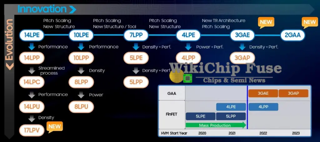
But Samsung's 5LPE process node's only roughly on par with TSMC's N7/N7P/N6 process node when the CPU frequency's ≤ 1.8 GHz. Samsung's 5LPE process node can consume up to 24% more power than TSMC's N7/N7P/N6 process node when the CPU frequency's > 1.8 GHz.
lattjeful
Like Like
- Pronouns
- he/him
I hope so. I’m just excited to see this thread alive again. I know enough to keep up with the more in depth discussion, but not enough to start any of it.So the real deal rumblings are starting to materialized, would you say it is a matter of weeks before we see the chip itself coming off the line, still warm?
I need something to read while I’m sitting at work doing nothing.
Goodtwin
Like Like
This remains unrealized, we also know that the GPU clock for Mariko goes as high as 1.267MHz offering 648GFLOPs, compared to OG's 393GFLOPs, the CPU also was similar enabled for higher clocks, short of 2GHz. This is likely the canceled Switch Pro model that Digital Foundry mentioned. It makes sense why the OLED model is so different even though the internal specs remain the same.
Being able to upscale properly to 4K thanks to a more capable dock and the addition of a "boost" mode using the higher clock speeds available with the Mariko X1 revision would have fit well with similar past revisions such as the DSi and New 3DS. As we have seen with jailbroken Switch units, increasing clock speeds does not require developers to do any patches, so it would just work. Nintendo may have seen this as a potential PR headache though, it wouldn't take long for people to realize that all V2 Switch units have the same processor and are capable of this Boost mode, but its locked behind a firmware update. They ultimately ended up concluding that it wasn't worth it and the straightforward OLED upgrade was easy for customers to understand and it has worked out for them. I stand by the idea that the dock having the ability to output 4K was originally intended for the Switch OLED. There is no reason for the Realtek chip to be in there otherwise. Its not in the standard Switch Dock, so its not a situation where sourcing that chip makes economical sense. If that were the case we would have seen it show up in the stand Switch dock as well as the OLED, but that isn't the case.
The 5nm Samsung rumor makes sense. Samsung was listed as the foundry in the NVN2 and since Orin is manufactured with Samnsung, it makes sense that Drake would be as well. What hasn't made sense with Drake is for it being 8nm like Orin. It needs a better process in order to make good use of those 12 Sm's. Samsung 5LPP is not cutting edge, and that is exactly why Nintendo/Nvidia would be in good position to negotiate a good price with Samsung. Power draw, performance and price was the primary criteria. Seems like a good match. 4N would be even better, but who was more likely to sharpen their pencil for a low cost SOC? TSMC with 4N or Samsung with 5LPP? Samsung has been struggling to keep up with TSMC for the past few years, seems like Samsung could use a high volume opportunity even if the margins arent great.
LiC
Member
Cache is smaller, faster memory which temporarily holds data that the GPU is using. It's faster both because of the memory type and because it's on-die, sharing circuit space with the CPU and/or GPU. Because the storage space is very small, the data in it has to be constantly juggled. The bigger the cache, the more likely that data for a given operation can stay in there and not need to be bounced back and forth from main memory (and/or VRAM in the case of a discrete graphics card), improving performance. Inefficient cache usage pushes you further away from the theoretical maximum GPU output because more time is spent waiting on data to come from memory before it can be processed.Sorry, I wasn’t wondering about like exact performance numbers.
I just am a dummy and was hoping someone could explain to me what L2 cache even is and how it is used/impacts something in like a video game console.
Like is 1 MB vs 4 MB a big deal? To me (a dummy) it seems like a lot!
Developers don't directly decide what goes into the cache (although they can perform some high-level operations like invalidating/flushing the entire thing). The best they can do is structure their code and data in such a way that it results in effective cache usage, with the help of performance profiling tools to see what the impact is. The more cache, the easier it is to do that. That said, entire games can be written without even paying attention to the cache -- it can just be a tricky optimization bottleneck, most likely to come up when dealing with tight performance constraints like in the porting of Witcher 3.
Concernt
Optimism is non-negotiable
- Pronouns
- She/Her
...where 1080p would still be a sweet spot for 7" and Samsung has huge OLED panel production capacity.screen resolution and sizes are a product of how they're fabbed. panels are cut akin to how chips are cut, so maximizing yields via panel size and pixel density would do more for costs than any particular panel being made a billion times over. unless you're buying leftovers like some of these handheld pcs are, you're doing custom orders
Concernt
Optimism is non-negotiable
- Pronouns
- She/Her
1080p OLED panels sip power, the difference between it and 720p aren't nothing, but they're not extremely significant either. The power consumption concerns with higher resolutions has more to do with how it takes more processing power to drive them at native res. Drake, however, has DLSS and what appears to be a very efficient node, so that isn't much a concern when games can still be rendering at 720p internally.Was the power requirements and resulting battery drain for 720p vs 1080p/IPS vs OLED panels discussed?
I'd personally have no problem with a 720p OLED screen recycled from the current OLED Switch, and was led to believe all this time that a 1080p screen in handheld mode would require more energy for a reduced return on investments in terms of performance compared to a 720p screen. Have efficiencies been developed that a 1080p screen would be viable after all, even if it the details would be lost unless you're holding the device four inches away from your face?

ReddDreadtheLead
#TeamLate2025WithAPotentialForEarly2026
- Pronouns
- He/Him
I would not use the term ”reputable” for someone like this lolSupposedly reputable, at least according to neo2046
This is honestly a case of someone saying something, and they say a lot of something….
Nintendo could have chosen more battery life with the OG switch if that’s the caseOf course, you are both right. However, I also operate on the assumption that Nintendo will want to maximize the battery life (like they have done so far). So I went with oldpuck's conservative assumption.
Cuzizkool
Shriekbat
- Pronouns
- He/Him
it probably has some life in it for refinement and long life for non-critical components
Yeah, Samsung's 5LPP process node is an evolution of Samsung's 7LPP process node.
But Samsung's 5LPE process node's only roughly on par with TSMC's N7/N7P/N6 process node when the CPU frequency's ≤ 1.8 GHz. Samsung's 5LPE process node can consume up to 24% more power than TSMC's N7/N7P/N6 process node when the CPU frequency's > 1.8 GHz.
So what I’m getting from this, especially the graphic, is that there could be a “5LPU” and/or “5LPV” in the future, that could be compatible with a Drake V2/Lite/Pro somewhere down the line, if Nintendo decided to take that route.
Since this is the top of this page, I want to detail some thoughts on the info we have so far.
The 5LPP Samsung node rumor from ~5 hours ago, found on the last page, offers a ~50% power consumption reduction over 8nm found in Orin.
There were clocks found in the Nvidia hack's NVN API, a DLSS test using an Ampere GPU, it had 3 clocks, 660MHz "4.3w", 1.125GHz "9.2w" and 1.38GHz "12w"...
- I believe these are 3 separate tests for 3 separate modes, "handheld", "docked" and "stress test"
- Handheld mode would offer 2TFLOPs (better than steam deck) + DLSS
- Docked mode would offer 3.456TFLOPs (same tier as Xbox Series S) + DLSS
- I tracked Orin's estimated power consumption via Nvidia's power estimation tools. 624MHz with Drake's configuration requires ~8.5w on 8nm, and the name of this DLSS test's clock was "4.3w", this lines up extremely well with the rumor that Drake is on 5LPP, these numbers are estimations, and the GPU is different, but it falls in the realistic range, as does 1.125GHz from what I've been able to extrapolate from the tool.
- Orin's CPU power consumption for 8 cores @ 1.881MHz is 4.5w, considering only 7 cores would be used for games, with one being reserved for the OS, this would give 3.94w on those 7 cores, and a reduction of power consumption to half is 1.97w. TX1 on 20nm was 1.83w for the 4 cores on A57 which could not be individually down clocked for the 4th core on the OS.
And from this handheld power, I’m guessing Drake can more than handle a 1080p screen.
- Pronouns
- He/Him/His
Ahh, okay, that does make more sense then. (I hope my following question makes sense) Would DLSS upscaling from 720p to a 1080p panel still offer better performance/battery life, rather than a native 720p rendering for a 720p panel or 360p/480p upscaled to 720p for the same panel?1080p OLED panels sip power, the difference between it and 720p aren't nothing, but they're not extremely significant either. The power consumption concerns with higher resolutions has more to do with how it takes more processing power to drive them at native res. Drake, however, has DLSS and what appears to be a very efficient node, so that isn't much a concern when games can still be rendering at 720p internally.
Hey hey, don't shoot the messengerI would not use the term ”reputable” for someone like this lol
This is honestly a case of someone saying something, and they say a lot of something….
 I'm only providing context when it was originally brought up in discussion haha (and if I'm being honest, I don't even know what it necessarily implies)
Last edited:
OP
OP
Not very likely based on Samsung's most recent roadmap.So what I’m getting from this, especially the graphic, is that there could be a “5LPU” and/or “5LPV” in the future, that could be compatible with a Drake V2/Lite/Pro somewhere down the line, if Nintendo decided to take that route.
AxkilAvenger
Like Like
- Pronouns
- He/him
I got a shit load of work to do everyday and understand none of the talk in this thread..yet I’m here multiple times a day..lurking…watching.I hope so. I’m just excited to see this thread alive again. I know enough to keep up with the more in depth discussion, but not enough to start any of it.
I need something to read while I’m sitting at work doing nothing.
not that simple as it varies between many companies and their process. I don't think I've ever seen a breakdown of different panel-makers yields and optimal sizes/resolutions...where 1080p would still be a sweet spot for 7" and Samsung has huge OLED panel production capacity.
Concernt
Optimism is non-negotiable
- Pronouns
- She/Her
Ahh, okay, that does make more sense then. (I hope my following question makes sense) Would DLSS upscaling from 720p to a 1080p panel still offer better performance/battery life, rather than a native 720p rendering for a 720p panel or 360p/480p upscaled to 720p for the same panel?
No, but it would look a lot better and have a similar power budget. 1080p DLSS with an internal Res of 720p would have higher image quality than native 720p. 1080p is also on the low end of where DLSS is effective, as the extreme low resolutions 720p would have as inputs would be more prone to artefacting and produce lower IQ.
It would appear that this device will indeed use DLSS even in handheld mode, and the very same tests that imply this do so to 1080p at 4W of power consumption, the same as the GPU of the original Switch in handheld mode. These power consumption tests line up with the leaked process node, 5LPP. As such, there is reason to believe that 1080p is the target for handheld mode, which makes much more sense for a 1080p panel.
Concernt
Optimism is non-negotiable
- Pronouns
- She/Her
It's never that simple, but understand that I AM choosing to simplifynot that simple as it varies between many companies and their process. I don't think I've ever seen a breakdown of different panel-makers yields and optimal sizes/resolutions

Kenka
Like Like
- Pronouns
- He/Him
Who is "We"? Because I'm not doing that. ZombI3 apparently isn't.
Nintendo did choose battery life in the Erista Switch. The Tegra X1 chip was (m)assively underclocked.Nintendo could have chosen more battery life with the OG switch if that’s the case
Concernt
Optimism is non-negotiable
- Pronouns
- She/Her
And Drake on 5LPP, targeting 2TF of performance, in handheld mode, would use 4W for its GPU. The same as the Tegra X1.Nintendo did choose battery life in the Erista Switch. The Tegra X1 chip was (m)assively underclocked.
Considering batteries have gotten better since 2017, and the power consumption is substantially the same, that sounds like "the same or better" battery life to me. Which seems reasonable, no?
Plus, the X1 was underclocked for thermal reasons too. With its cooling system it COULD have clocked higher (in TV Mode), but then you risk making the dock a Switch toaster. Even if the console can't take that, little kids being burned would be a bad look. Let's not forget the Tegra X1 on 20nm MOSFET was... Pretty terrible, heat dissipation wise.
CullenLX87
Cappy
- Pronouns
- He/Him
I got a shit load of work to do everyday and understand none of the talk in this thread..yet I’m here multiple times a day..lurking…watching.
ReddDreadtheLead
#TeamLate2025WithAPotentialForEarly2026
- Pronouns
- He/Him
The OG doing at worst 2 hours in a game is not choosing battery life lolNintendo did choose battery life in the Erista Switch. The Tegra X1 chip was (m)assively underclocked.
Concernt
Optimism is non-negotiable
- Pronouns
- She/Her
An interesting question. Was Switch with the X1 clocked as low as it could go in its power curve before efficiency dropped off, when in handheld (or tabletop) mode?The OG doing at worst 2 hours in a game is not choosing battery life lol
ItWasMeantToBe19
Manakete
What resolution would be retina level for a device with a screen size of the Switch (obviously this requires assumptions on how far away people hold their Switch from their eyes)
- Pronouns
- He/Him
Switch is technically "retina" level as is.What resolution would be retina level for a device with a screen size of the Switch (obviously this requires assumptions on how far away people hold their Switch from their eyes)
the lowest "retina display" ppi is like 220 ppi. the 7in 720p is 209 ppi. so the OG switch and the lite are already a retina displayWhat resolution would be retina level for a device with a screen size of the Switch (obviously this requires assumptions on how far away people hold their Switch from their eyes)
- Pronouns
- he / him
Seems like a surprisingly small gap between docked and undocked, especially given the potential resolution gap is greater this time around, barring a 1440p screen.There were clocks found in the Nvidia hack's NVN API, a DLSS test using an Ampere GPU, it had 3 clocks, 660MHz "4.3w", 1.125GHz "9.2w" and 1.38GHz "12w"...
- I believe these are 3 separate tests for 3 separate modes, "handheld", "docked" and "stress test"
- Handheld mode would offer 2TFLOPs (better than steam deck) + DLSS
- Docked mode would offer 3.456TFLOPs (same tier as Xbox Series S) + DLSS
If those were the main modes and handheld was doing 1080p DLSS while docked was doing 4K DLSS, the pre-DLSS render resolution probably wouldn't be much greater docked than undocked.
Probably only makes a migration speed difference if they have MASSIVE production for that first year or so, enough that it wouldn't all sell out at ~400 anyway.Yeah, I admit that. But imagine how quickly Nintendo will be able to build a userbase at this price! We would have a shorter migration window and more incentives for developers to come up quickly with exclusive titles.
ItWasMeantToBe19
Manakete
How much of an actual improvement would 1080p be from 720p in terms of visual experience (assuming literally no drawbacks in terms of power draw just for the sake of argument)
SoldierDelta
Designated Xenoblade Loremaster
- Pronouns
- he/him
I can't claim to be an expert, but the general idea would be a better pixel density and the potential to make the device larger without having a smaller density than the original Switch's. Both meaning a clearer image.How much of an actual improvement would 1080p be from 720p in terms of visual experience (assuming literally no drawbacks in terms of power draw just for the sake of argument)
I don't know the consensus, but I don't think it'd be a good idea for Nintendo to opt for a 1080p for their next device. If they can keep a high battery life and low cost, then sure they could do it. I just don't think the trade-off would be worth it, especially since it'd either mean trading off the OLED screen, increasing the price or investing in a much more powerful battery.
ReddDreadtheLead
#TeamLate2025WithAPotentialForEarly2026
- Pronouns
- He/Him
I’m not familiar with its total curvature so I can’t answer that, but if it was clocked lower it would be more fine with regards to the bandwidth it has. Like clocking the switch higher doesn’t solve the bandwidth limitation it has to it, as seen by Bayonetta 3. It just makes it more obvious that it’s limited regardless.An interesting question. Was Switch with the X1 clocked as low as it could go in its power curve before efficiency dropped off, when in handheld (or tabletop) mode?
RennanNT
Bob-omb
I will use an analogy to make it easier to understand the general idea of how it works:I just am a dummy and was hoping someone could explain to me what L2 cache even is and how it is used/impacts something in like a video game console.
Imagine someone who works reading and writing documents the whole day. These documents are stored in another room of the building.
Going back and forth to that storage room takes too much time, so the worker bring huge stacks of documents every time they go to the storage and put those docs in shelves on their office.
To not waste much time getting up and going to these shelves either, they get a stack of what they're likely working next on and put it in their desk's drawers.
The worker is the CPU/GPU.
The storage room is the HDD/SDD.
The shelves is the RAM.
The drawers is the Cache.
The amount of documents you can move to/from at once is the bandwidth.
In short, the RAM and cache systems are there to minimize the time spent waiting data, making the CPU and GPU more productive. OTOH, you don't want to go overkill, as you're spending money which would get you better results being spent elsewhere. So finding the right amount is a balancing act based on the rest of the system.
Oh, and there are multiple levels of cache, L2 being the second level and is slower but bigger in capacity when compared to the L1.
Threadmarks
View all 18 threadmarks
Reader mode
Reader mode
Recent threadmarks
Poll #3: When do you think is the launch window for Nintendo's new hardware? Announcement regarding links to news and rumours from 2022 and 2021 Rough summary of the 2 August 2023 episode of Nate the Hate Rough summary of the 11 September 2023 episode of Nate the Hate Anatole's deep dive into a convolutional autoencoder Differences between T234 and T239 Rough summary of the 19 October 2023 episode of Nate the Hate necrolipe's Twitter (X) post on why a 2025 launch doesn't automatically make T239 outdated based on one of the leaked slides from Microsoft
Staff Communication
View all 12 threadmarks
Reader mode
Reader mode
Recent threadmarks
Regarding Hogwarts Staff Communication 05/26/23 Staff Post about Citing Leaks and Rumors Staff Post about reading Hidden Content Staff Post- Please read Keeping on topic New Switch 2 ST Made - Nontechnical Talk Has A New Home Staff Post Regarding Dubious Insiders And Better SourcingPlease read this staff post before posting.
Furthermore, according to this follow-up post, all off-topic chat will be moderated.
Furthermore, according to this follow-up post, all off-topic chat will be moderated.
Last edited: