• Hey everyone, staff have documented a list of banned content and subject matter that we feel are not consistent with site values, and don't make sense to host discussion of on Famiboards. This list (and the relevant reasoning per item) is viewable here.
  • Do you have audio editing experience and want to help out with the Famiboards Discussion Club Podcast? If so, we're looking for help and would love to have you on the team! Just let us know in the Podcast Thread if you are interested!

StarTopic Future Nintendo Hardware & Technology Speculation & Discussion |ST| (Read the staff posts before commenting!)

Since this is the top of this page, I want to detail some thoughts on the info we have so far.

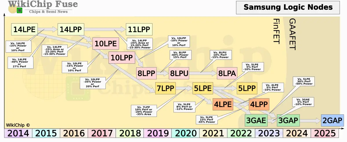
The 5LPP Samsung node rumor from ~5 hours ago, found on the last page, offers a ~50% power consumption reduction over 8nm found in Orin.

There were clocks found in the Nvidia hack's NVN API, a DLSS test using an Ampere GPU, it had 3 clocks, 660MHz "4.3w", 1.125GHz "9.2w" and 1.38GHz "12w"...
  • I believe these are 3 separate tests for 3 separate modes, "handheld", "docked" and "stress test"
  • Handheld mode would offer 2TFLOPs (better than steam deck) + DLSS
  • Docked mode would offer 3.456TFLOPs (same tier as Xbox Series S) + DLSS
  • I tracked Orin's estimated power consumption via Nvidia's power estimation tools. 624MHz with Drake's configuration requires ~8.5w on 8nm, and the name of this DLSS test's clock was "4.3w", this lines up extremely well with the rumor that Drake is on 5LPP, these numbers are estimations, and the GPU is different, but it falls in the realistic range, as does 1.125GHz from what I've been able to extrapolate from the tool.
  • Orin's CPU power consumption for 8 cores @ 1.881MHz is 4.5w, considering only 7 cores would be used for games, with one being reserved for the OS, this would give 3.94w on those 7 cores, and a reduction of power consumption to half is 1.97w. TX1 on 20nm was 1.83w for the 4 cores on A57 which could not be individually down clocked for the 4th core on the OS.

Thanks to Thraktor's digging, OLED model seems to have been designed to output 4K image, possibly via upscaling (non-tensor core accelerated). This remains unrealized, we also know that the GPU clock for Mariko goes as high as 1.267MHz offering 648GFLOPs, compared to OG's 393GFLOPs, the CPU also was similar enabled for higher clocks, short of 2GHz. This is likely the canceled Switch Pro model that Digital Foundry mentioned. It makes sense why the OLED model is so different even though the internal specs remain the same.

They would eventually need one to make a Lite, and offer an entry level SKU.
That isn't needed IMO. If they keep the same battery, and use a more advanced RAM and smaller screen, they could reach 4 hours instead 3.5 hours... which is in line with Switch Lite's ~3 hours minimum, where OG Switch is 2.5 hours minimum (3 in Zelda).
 
Last edited:
If it was 8nm, it would have been 1.3TFLOPs and the CPU would have likely been 1.2-1.4GHz.
5nm LPP should offer ~60% higher clocks for both GPU and CPU... TSMC 5nm would have offered as much as 75% higher clocks.
Do we have actual numbers for the performance of Samsung 5LPP? I thought 5LPE was the one we had solid information about?

If so, it'd be good to bring those numbers all up again, especially in comparison to 5LPE, which is the node people first think of when thinking of Samsung 5nm, even though 5LPP is by definition a better node (assuming it meets its performance targets). I remember @Thraktor's post from a few months ago, but I don't have the time to find it at the moment.

Edit: That edit in the above post is definitely a helpful summary of what the node brings to the table, assuming the clocks in the Nvidia hack are what will be available in the final product.
 
Last edited:
Do we have actual numbers for the performance of Samsung 5LPP? I thought 5LPE was the one we had solid information about?

If so, it'd be good to bring those numbers all up again, especially in comparison to 5LPE, which is the node people first think of when thinking of Samsung 5nm, even though 5LPP is by definition a better node (assuming it meets its performance targets). I remember @Thraktor's post from a few months ago, but I don't have the time to find it at the moment.

Edit: That edit in the above post is definitely a helpful summary of what the node brings to the table, assuming the clocks in the Nvidia hack are what will be available in the final product.
Yes, it's still speculation what those clocks are, but it's hard to ignore them and they do fit with the power consumption we are seeing.
wikichip-samsung-q2-2022-roadmap.png

Thanks to @Zedark 's post, we can figure that out pretty quickly... It's important to note that these numbers are all advertised estimations, but here is my math anyways, it all starts from 10LPP:
1w 10LPP -35% 7LPP -20% 5LPE -10% 5LPP = ~47%
1w 10LPP -10% 8LPP = 90%
Thus, 5LPP Samsung is about half of 8LPP Samsung, which Orin uses.
 
If Drake is using 5LPP, and the clocks found in the DLSS tests are approximate to the final clocks then I am struggling to see Nintendo using a 720p panel.

I imagine most developers programming for [REDACTED] are going to opt to use DLSS any place they can, with 2 TFLOPS plus DLSS in handheld to play with a 720p - 1080p DLSS image will look incredibly impressive on a 7 inch display, to the point where the IQ may make handheld play preferable to docked in some instances. For more demanding games 540p - 1080p DLSS could be used and still produce an image that looks superior to a native 720p render for a likely reduced performance hit.

The question then is, will it be a 1080p OLED Panel? Unfortunately 1080p 7 inch LCD panels appear to be far more prevalent than OLED ones, so depending on the price point Nintendo wants to launch this, I can see it being an IPS panel. Hope Nintendo proves me wrong and managed to snag a nice package deal with Samsung that includes their OLED panels.

Actually, one thing I hadn't considered is that they could opt for a Samsung QLED panel as a middle ground. The average consumer likely wouldn't know the difference and not see it as a downgrade.
 
Last edited:
720p are in my opinion enough to get an image quality Nintendo, and myself, would be happy with. And if there's power to spare, downsampling a higher resolution image would look great in any case.
However, I've recently warmed up to the idea of a 1080p screen just because it's a low hanging fruit for Nintendo to promote an improvement as compared to the Switch, and avoid the "who wants to game in 720p in 2024?" narrative.
 
If Drake is using 5LPP, and the clocks found in the DLSS tests are approximate to the final clocks then I am struggling to see Nintendo using a 720p panel.

I imagine most developers programming for [REDACTED] are going to opt to use DLSS any place they can, with 2 TFLOPS plus DLSS in handheld to play with a 720p - 1080p DLSS image will look incredibly impressive on a 7 inch display, to the point where the IQ may make handheld play preferable to docked in some instances. For more demanding games 540p - 1080p DLSS could be used and still produce an image that looks superior to a native 720p render for a likely reduced performance hit.

The question then is, will it be a 1080p OLED Panel? Unfortunately 1080p 7 inch LCD panels appear to be far more prevalent than OLED ones, so depending on the price point Nintendo wants to launch this, I can see it being an IPS panel. Hope Nintendo proves me wrong and managed to snag a nice package deal with Samsung that includes their OLED panels.

Actually, one thing I hadn't considered is that they could opt for a Samsung QLED panel as a middle ground. The average consumer likely wouldn't know the difference and not see it as a downgrade.
Kinda hope Nintendo uses IPS 1080p panel to save some costs. I have OLED monitors and IPS and while it is a nice difference I don't mind it when compared to a very nice IPS plus it will allow Nintendo to come out with switch redacted OLED in the future
 
Kinda hope Nintendo uses IPS 1080p panel to save some costs. I have OLED monitors and IPS and while it is a nice difference I don't mind it when compared to a very nice IPS plus it will allow Nintendo to come out with switch redacted OLED in the future
The screen would have to bring obvious improvements in brightness (plus, say, HDR capability) and satisfactory black levels for Nintendo to sell it as an upgrade. I just don’t see them releasing a new premium handheld with a screen that is not an objective improvement over the one in a previous generation console.
 
720p are in my opinion enough to get an image quality Nintendo, and myself, would be happy with. And if there's power to spare, downsampling a higher resolution image would look great in any case.
However, I've recently warmed up to the idea of a 1080p screen just because it's a low hanging fruit for Nintendo to promote an improvement as compared to the Switch, and avoid the "who wants to game in 720p in 2024?" narrative.
Steam Deck is popular in online discussion and uses 800p, the 16:10 equivalent of 720p. If the device underneath is powerful enough, enthusiasts won't care. The only reason to hope for 1080p over 720p is imo VRR in handheld mode, which would be great for titles with uneven framerates. Even in that case, though, the performance overhead gained with a 720p res would be enough to smooth that out
 
If Drake is using 5LPP, and the clocks found in the DLSS tests are approximate to the final clocks then I am struggling to see Nintendo using a 720p panel.

I imagine most developers programming for [REDACTED] are going to opt to use DLSS any place they can, with 2 TFLOPS plus DLSS in handheld to play with a 720p - 1080p DLSS image will look incredibly impressive on a 7 inch display, to the point where the IQ may make handheld play preferable to docked in some instances. For more demanding games 540p - 1080p DLSS could be used and still produce an image that looks superior to a native 720p render for a likely reduced performance hit.

The question then is, will it be a 1080p OLED Panel? Unfortunately 1080p 7 inch LCD panels appear to be far more prevalent than OLED ones, so depending on the price point Nintendo wants to launch this, I can see it being an IPS panel. Hope Nintendo proves me wrong and managed to snag a nice package deal with Samsung that includes their OLED panels.

Actually, one thing I hadn't considered is that they could opt for a Samsung QLED panel as a middle ground. The average consumer likely wouldn't know the difference and not see it as a downgrade.
Panels are made to order. Making a 1080p oled panel isn't a problem.

That's said all that excess power can be used elsewhere, like ray tracing, dlaa, whatever
 
Steam Deck is popular in online discussion and uses 800p, the 16:10 equivalent of 720p. If the device underneath is powerful enough, enthusiasts won't care. The only reason to hope for 1080p over 720p is imo VRR in handheld mode, which would be great for titles with uneven framerates. Even in that case, though, the performance overhead gained with a 720p res would be enough to smooth that out
I would love VRR.

Also, Paranoia Agent. :love:
 
What sort of timeline do we think us likely. Assuming this 5 LPP is true, are we assuming production has started or will start soon ?
still hard to say. this all depends on when Nintendo is ready to begin the process. if they want to launch before the end of the FY, then production will probably start late summer
 
still hard to say. this all depends on when Nintendo is ready to begin the process. if they want to launch before the end of the FY, then production will probably start late summer.
From the rumors around production, as well as the knowledge that T239 is physically ready for mass production, it will start sometime in the next 3 to 7 months, and launch sometime in November 2023 - March 2024. Anything beyond that date, puts into question why the SoC was completed so early, stale designs tend to cost more.
 
I would love VRR.

Also, Paranoia Agent. :love:
I'm glad someone finally noticed!

EDIT: To keep things on track here, personally my prediction is that Nintendo will stick with 720p screens with the Switch 2, maybe even LCD so they double dip on people wanting a more premium-feeling experience
 
I don't see them going back to LCD until they do a Lite model. the hybrid is definitely gonna cost more than the mariko OLED model, so they wouldn't go with less premium screen
 
Can't they just support VRR in docked mode and leave it disabled in portable assuming it aims for native 720p60 there?
(as long as the connected display supports VRR)
 
Last edited:
0
I don't see them going back to LCD until they do a Lite model. the hybrid is definitely gonna cost more than the mariko OLED model, so they wouldn't go with less premium screen
VRR + HDR are basically the only way I could see them marketing an LCD screen as a premium feature. Sadly I don’t see them shelling out MiniLED tech.
 
My hunch for 720p is that it is enough. They may go with 800p like the deck for a true 16:9

Also if they are ordering millions of screens for the OLED already it would be much cheaper to reuse that part.
 
My hunch for 720p is that it is enough. They may go with 800p like the deck for a true 16:9

Also if they are ordering millions of screens for the OLED already it would be much cheaper to reuse that part.
the Steam Deck is 16:10. with how much people complain about bezels, this gives an artificial bezel if you don't fill the screen

VRR + HDR are basically the only way I could see them marketing an LCD screen as a premium feature. Sadly I don’t see them shelling out MiniLED tech.
harder to market I think. "VRR" isn't common parlance outside enthusiast communities
 
In the case anyone would be asking, nodes don't make a device more or less powerful. They determine largely how much energy they sip to function.
And yes, if you're wondering, we are still projecting that this device will deliver between 1.4 to 2.3 TFLOPS, which is Playstation 4 territory.


GPU: Nvidia Ampere with 1536 CUDA cores (12 SMs/6 TPCs)
  • Original Switch Clocks seem likely, 460MHz/768Mhz, for 1.4/2.3 TFLOPS
 
What sort of timeline do we think us likely. Assuming this 5 LPP is true, are we assuming production has started or will start soon ?

The one and only, soon to be official timeline:

The soon to be official timeline:

1. Zelda releases on the OG switch, please enjoy.
2. The next console is finally mentioned by Nintendo at E3. Planned for 2024. "We're always looking for new ways to satisfy our fans and deliver the best possible switch experience. As technology advances, so does the Switch" . To the surprise of no one, it's another Switch.

3. Drip feeding of info until the holidays. Devs start talking, YouTubers make annoying faces on their videos, and insiders try to convince their fans that they predicted everything. In the meantime, Nintendo wants people to continue buying the current Switch during the holidays and reassure everyone that it won't suddenly die when Switch 2 releases.

4. General presentation of the new console around January 2024. It's Drake on a node better than fucking 8nm Samsung. Mario is an exclusive launch title, first trailer of Mario Kart 9 (June 2024). We also see the Zelda DLC and holy shit does it look good on Drake.

5. The new console releases in April 2024.

6. Nintendo lied and the OG Switch is cerebrally dead by October, because the new console is just SO MUCH better.

And you are welcome.
 
In the case anyone would be asking, nodes don't make a device more or less powerful. They determine largely how much energy they sip to function.
And yes, if you're wondering, we are still projecting that this device will deliver between 1.4 to 2.3 TFLOPS, which is Playstation 4 territory.


GPU: Nvidia Ampere with 1536 CUDA cores (12 SMs/6 TPCs)
  • Original Switch Clocks seem likely, 460MHz/768Mhz, for 1.4/2.3 TFLOPS
We have clocks that exist in NVN for Ampere that are impossible on 8LPP, but do match up with 5LPP, which further connects those clocks as target clocks for the GPU. 660MHz in handheld (2TFLOPs) and 1.125GHz docked (3.456TFLOPs) in addition to these raw numbers, we can add DLSS to allow the GPU to do more with less, greatly outstripping the PS4 even in the handheld mode.
 
As I've mentioned before, Nintendo's and Nvidia's decision to have Drake's GPU have 1 MB of L2 cache instead of 4 MB of L2 cache like with Orin's GPU makes more sense with Samsung as the foundry partner for reasons explained here.
How much would Nintendo settling for 1 MB of L2 cache instead of 4 MB impact or negatively affect its processing speed potential?

Is this something developers would be frustrated by the lack of or would it be easy to work around? What types of things would it specifically impact in a game engine?
 
Quoted by: LiC
1
How much would Nintendo settling for 1 MB of L2 cache instead of 4 MB impact or negatively affect its processing speed potential?

Is this something developers would be frustrated by the lack of or would it be easy to work around? What types of things would it specifically impact in a game engine?
Nobody here knows the answer to that. All specs in a chip/system are made for balance. Whatever final number is used will be a compromise between performance and cost/heat/size/etc. like all other the numbers.
 
I would love VRR.

Also, Paranoia Agent. :love:
Wait how’d you get PA from that post?😭
In the case anyone would be asking, nodes don't make a device more or less powerful. They determine largely how much energy they sip to function.
And yes, if you're wondering, we are still projecting that this device will deliver between 1.4 to 2.3 TFLOPS, which is Playstation 4 territory.


GPU: Nvidia Ampere with 1536 CUDA cores (12 SMs/6 TPCs)
  • Original Switch Clocks seem likely, 460MHz/768Mhz, for 1.4/2.3 TFLOPS
There’s an indirect correlation and a correlation that matters. If it’s less efficient, and produces more heat by being on a worse node, and they have to compromise for this not only for the safety of the silicon and the product but also the performance of the system, then yes the node does impact how powerful it can be in this case.

If we are looking at it from a size perspective, then this doesn’t have anything to do with performance.

Also, with respect to those numbers, it keeps on getting brought up, but that’s just a floor of expectations, it is not the ceiling of what they can achieve.
 
In the case anyone would be asking, nodes don't make a device more or less powerful. They determine largely how much energy they sip to function.
And yes, if you're wondering, we are still projecting that this device will deliver between 1.4 to 2.3 TFLOPS, which is Playstation 4 territory.


GPU: Nvidia Ampere with 1536 CUDA cores (12 SMs/6 TPCs)
  • Original Switch Clocks seem likely, 460MHz/768Mhz, for 1.4/2.3 TFLOPS
It can also mean more power for the same battery and for the same size 😉
 
I wonder if Nintendo can hit the magical 299 USD price point at the Drake launch. Would be fantastic.
Launching for fewer dollars than OLED did in 2021 is really really dreaming.
I'm currently trying to get my mother to download Stella Glow on my 3ds that I have at her house because some company that is completely normal just decided to shut down the 3ds and WiiU eshop.
If you think of anything else you want to buy, might be simpler to cut out the middlemom and just buy it online, then download it whenever you have the 3DS with you.
 
Does anyone have a (link to a) map/explanation of the different process nodes and how they compare in terms of density and performance (in a quantitative sense)? Might be useful for perspective in case this person is legit (don't know of them, but I don't follow the mobile phone scene at all, so that means literally nothing).

Edit: Also, how does 5LPP compare to 5LPE? I can't find even a mention of 5LPP anywhere on Google, let alone solid numbers...

Edit 2: This might help:
wikichip-samsung-q2-2022-roadmap.png


I've found 5LPE roughly matches 7nm TSMC, as well.
5% higher performance at the same power for Samsung's 5LPP process node (vs Samsung's 5LPE process node).
Although there's so much interesting topics and information in the SemiAnalysis article, I'm only going to quote a section from the SemiAnalysis article that's likely the most relevant with respect to Nintendo's new hardware.

And Samsung's 5LPE process node's only roughly on par with TSMC's N7/N7P/N6 process node when the CPU frequency is ≤ 1.8 GHz. Samsung's 5LPE process node can consume up to 24% more power than TSMC's N7/N7P/N6 process node when the CPU frequency's > 1.8 GHz.
 
Those clocks weren't in NVN or for Ampere.
You found it, you tell us why you thought they were connected to Nintendo.
LiC said:
the test has a lot of automation to it. it auto-builds NVN and the test app. I think it even auto-pulls the source to make sure DLSS is up to date
This was how you explained it to me. Also Nvidia SoC can run windows now.
 
Last edited:
TLDR: The original Switch wasn't physically capable of outputting 4K via its USB-C port, but Nintendo made specific changes to the motherboard of the OLED model to support 4K output. We already know that the OLED dock was also upgraded with hardware capable of 4K output. Software changes relating to 4K output were also added to the OS alongside support for this hardware. Therefore, I believe that the Switch OLED model is the elusive Switch Pro/Switch 4K, and that they only decided to drop 4K support and higher clocks at a late stage after the hardware had been finalised.
Thank you for this breakdown!

I was hoping that if video streaming apps did make their way to Switch, that 4K output would be possible for an original model if it were sitting in an OLED dock, but I guess that was a foolish dream. Still, at least it saved me from buying an extra dock that wouldn't have had any real benefits for the V1 console.
 
Is Samsung 5LPP a dead end node? Or can it be shrunk? Im asking out of curiosity. There may or may not be a Drake Pro down the line, I just want to know if it’s feasible.
 
Please read this staff post before posting.

Furthermore, according to this follow-up post, all off-topic chat will be moderated.
Last edited:


Back
Top Bottom