• Hey everyone, staff have documented a list of banned content and subject matter that we feel are not consistent with site values, and don't make sense to host discussion of on Famiboards. This list (and the relevant reasoning per item) is viewable here.
  • Do you have audio editing experience and want to help out with the Famiboards Discussion Club Podcast? If so, we're looking for help and would love to have you on the team! Just let us know in the Podcast Thread if you are interested!

StarTopic Future Nintendo Hardware & Technology Speculation & Discussion |ST| (Read the staff posts before commenting!)

Apple matched that in 2018 in portable, Dane should have the benefit of being able to dock and have active cooling
passively cooled and paper specs mean jack shit. which has always been the problem with apple devices. RAM limited and eschewing fans mean a very weird perf profiles.
the NBA 2K they used to show off is clean but visually doesn't look good.
 
passively cooled and paper specs mean jack shit. which has always been the problem with apple devices. RAM limited and eschewing fans mean a very weird perf profiles.
the NBA 2K they used to show off is clean but visually doesn't look good.
My point is that it shouldn’t be difficult for Dane to do the same thing :p.

It has more modern features and has benefits that the A12Z or X or whatever don’t have to their disposal.
There would have already been talks about Dane being fabricated using a 7 nm** process node if that's actually the case. But that hasn't been the case. In fact, kopite7kimi has consistently said that Orin's using Samsung's 8N process node since the beginning of this year (here, here, and here). kopite7kimi also said that Dane's a custom variant of Orin. And I don't expect Dane to be heavily different from Orin, outside of using the Cortex-A78C instead of the Cortex-A78AE, and removing all of the hardware features Nintendo has no use for (e.g. safety island, programmable vision accelerators (PVA), etc.).

Also, securing enough capacity for any particular process node is a process that realistically takes companies to make plans a couple of years in advance. That's the reason why there's been talks about Hopper being fabricated using TSMC's 5 nm** process node over a year ago.

I think the implied "Nintendo is 100% doomed if Nintendo doesn't use the most cutting-edge process nodes" sentiment from some people is getting really old. Process nodes alone aren't enough to ensure optimal performance and power efficiency. Architecture design is at least equally as important.
I think that it’ll be fine, 8N is a variant of the 10nm process but it only came out recently ;). 8LPx are older already, but 8N wasn’t available until now last year and only one customer is allowed to use it because it was made specifically for and by then for their use case.

Cutting edge also doesn’t always mean the best, just that it’s relatively new. Switch was more cutting edge when it released despite being weaker as a platform.


wait what. I think I had auto correct. I meant to say it would be sad. Yeah a 720p xbone handheld experience is just a tad higher than 393 Maxwell GFLOPs.
I question if they fully did. We don't see games that fully hit the mark, just in bits and pieces
Apple’s metrics are off because it’s mostly useless, but it was more pointing that it shouldn’t really be difficult for Dane if that can apparently do similar to the XB1.


A better GPU architecture than what is in the 12Z/X. More efficient I think too.
 
I think it’s safe to say that Switch 2 will be power wise around 0.5Tf undocked and 1Tf docked with 8GB ram ( safest bet ).

I would love it if it was 1Tf undocked and 1.8Tf docked with 12GB ram
 
I think it’s safe to say that Switch 2 will be power wise around 0.5Tf undocked and 1Tf docked with 8GB ram ( safest bet ).
in pure flops, I don't think that's possible in a practical sense. even with 256 ampere cores on 8nm, you'd have such a high clock ceiling that you can hit 1TF easily
 
I think that it’ll be fine, 8N is a variant of the 10nm process but it only came out recently ;). 8LPx are older already, but 8N wasn’t available until now last year and only one customer is allowed to use it because it was made specifically for and by then for their use case.

Cutting edge also doesn’t always mean the best, just that it’s relatively new. Switch was more cutting edge when it released despite being weaker as a platform.
I agree. But I wouldn't be surprised if some people thought otherwise.

Also, no one knows for certain how Samsung's 8N process node compares with Samsung's 8LPP process node or Samsung's 8LPU process node when mobile SoCs are concerned. (I'm not talking about laptop GPUs by the way.) And I wouldn't be surprised if no one ever knows.
 
0
I know we're comparing apples and organs here but X1 at 20nm was fairly old even by 2017 standards and the speculation was Nintendo's nvidia deal included a sweet price on the SoC as they soaked up unused 20nm capacity.
So I don't think the stars will align again and they may indeed go for a newer process comparatively speaking for Switch 2, but assuming they stick with 8nm how much more dense is the Samsung 8nm compared to the old TSMC 20nm?

I think's its reaosnable to work backwards that way to see if it fits with the transitor count needed to hit a specific perf target. That will probably be more crucial than divining if Nintendo will splurg of a newer process because hoping for them to do that to eek out a bit more powerful hardware seems to always end in disappointment.
 
I know we're comparing apples and organs here

will-ferrel-say-what.gif
 
I know we're comparing apples and organs here but X1 at 20nm was fairly old even by 2017 standards and the speculation was Nintendo's nvidia deal included a sweet price on the SoC as they soaked up unused 20nm capacity.
So I don't think the stars will align again and they may indeed go for a newer process comparatively speaking for Switch 2, but assuming they stick with 8nm how much more dense is the Samsung 8nm compared to the old TSMC 20nm?

I think's its reaosnable to work backwards that way to see if it fits with the transitor count needed to hit a specific perf target. That will probably be more crucial than divining if Nintendo will splurg of a newer process because hoping for them to do that to eek out a bit more powerful hardware seems to always end in disappointment.
~13-16MTr/mm^2 I think for 22-20nm vs ~55-60MTr/mm^2 for 10/8nm

I’m ignoring that comparison incident lol
 
0
I know we're comparing apples and organs here but X1 at 20nm was fairly old even by 2017 standards and the speculation was Nintendo's nvidia deal included a sweet price on the SoC as they soaked up unused 20nm capacity.
So I don't think the stars will align again and they may indeed go for a newer process comparatively speaking for Switch 2, but assuming they stick with 8nm how much more dense is the Samsung 8nm compared to the old TSMC 20nm?

I think's its reaosnable to work backwards that way to see if it fits with the transitor count needed to hit a specific perf target. That will probably be more crucial than divining if Nintendo will splurg of a newer process because hoping for them to do that to eek out a bit more powerful hardware seems to always end in disappointment.
The Tegra X1 has ~2 million transistors and has a die size of ~118 mm², which translates to a transistor density of ~16.949 MTr/mm². And the Apple A8 also has ~2 billion transistors and has a die size of 89 mm², which translates to a transistor density of ~22.472 MTr/mm². So I think TSMC's 20 nm** process node has a transistor density of ~23 MTr/mm².

In comparison, Samsung mentioned that Samsung's 8LPP process node has a transistor density of 61.18 MTr/mm². Of course, I don't know how Samsung's 8LPU process node or Samsung's 8N process node compares to Samsung's 8LPP process node in terms of transistor density.
 
0
I think battery life is important, but I can foresee it hitting the same or similar targets to the 2017 OG Switch. It’s not amazing, but also not embarrassing, as evidenced by the ~38-40 million people who bought a Switch prior to the Mariko revisions released in and around August and September of 2019.
 
I'd also add that by targeting Dane V1 towards Erista's battery life, Nintendo can have some wiggle rooms to release Dane V2 made on denser litho with better battery life in the future.
 
I'd also add that by targeting Dane V1 towards Erista's battery life, Nintendo can have some wiggle rooms to release Dane V2 made on denser litho with better battery life in the future.
It’s a bit difficult to target exactly the same situation that Erista had though to be fair, it was on a less efficient mode that everyone moved on from quickly because it had heating issues. And the uArch for the A57 are less efficient than the A78 several fold. A57 ass their first foray into an 8core working and it didn’t work right. By the A75 it was functioning better with the newer uArch to make use of DynamIQ properly.

Though this also depends on the config, but they’d have to push it quite a bit to have such a low battery life imo.


Then again, you said targeting, not necessarily matching. I think they’ll have something that is like the Switch Lite in batter life, it’s slightly better than the V1, but worse than the V2.
 
0
I think battery life is important, but I can foresee it hitting the same or similar targets to the 2017 OG Switch. It’s not amazing, but also not embarrassing, as evidenced by the ~38-40 million people who bought a Switch prior to the Mariko revisions released in and around August and September of 2019.
I think it depends on if Nintendo's okay with a battery life range of 2.5 - 6.5 hours for the DLSS model*. Hypothetically, Nintendo could have kept the Nintendo Switch (2019)'s battery life range the same as the Nintendo Switch (2017), but increase the CPU, GPU, and RAM frequencies. However, Nintendo ultimately kept the Nintendo Switch (2019)'s CPU, GPU, and RAM frequencies the same, which resulted in a ~36.46% - 80% increase in battery life compared to the Nintendo Switch (2017). I think that might be an indication that Nintendo might not be okay with a battery life range of 2.5 - 6.5 hours.
 
I do find this article on the whole Samsung win of the Tesla HW 4.0 insightful and maybe slightly a little confusing to be honest on Nvidia's end of going with possibly 8nm for Orin. It definitely comes across like Samsung were extremely aggressive in negotiating this win and who knows maybe Nvidia taking the bulk of their business back to TSMC is what sparked this (Qualcomm as well).

There not being a clear indication of the manufacturing process for Orin in any article written is head scratching since any of the recent Tesla HW 4.0 and Samsung articles all mention them being made on Samsung's 7nm. The Tesla Ai event being back in August was well ahead of Nvidia's GTC November event and we now have full specs for both chips.

This quote below in of itself would be the most weird for Nvidia in still choosing 8nm if that pans out. The Tesla 4.0 chip is supposed to be a 645mm², 400w 22Tflop FP32 SoC on Samsung's 7nm process (according to the Tesla team in the video).

"Samsung Electronics plans to mass produce the Tesla HW 4.0 chip at its main Hwasung plant in Korea using the 7-nanometer processing technology in the fourth quarter of this year at the earliest, according to the sources.

The 7 nm process is less advanced than its 5 nm process, but Samsung has decided to use the 7 nm technology to ensure higher production yields and stable functions of the chip when installed on full self-driving (FSD) cars, they said."


Last edited:
I do find this article on the whole Samsung win of the Tesla HW 4.0 insightful and maybe slightly a little confusing to be honest on Nvidia's end of going with possibly 8nm for Orin. It definitely comes across like Samsung were extremely aggressive in negotiating this win and who knows maybe Nvidia taking the bulk of their business back to TSMC is what sparked this (Qualcomm as well).

There not being a clear indication of the manufacturing process for Orin in any article written is head scratching since any of the recent Tesla HW 4.0 and Samsung articles all mention them being made on Samsung's 7nm. The Tesla Ai event being back in August was well ahead of Nvidia's GTC November event and we now have full specs for both chips.

This quote below in of itself would be the most weird for Nvidia in still choosing 8nm if that pans out. The Tesla 4.0 chip is supposed to be a 645mm², 400w 22Tflop FP32 SoC on Samsung's 7nm process (according to the Tesla team in the video).

"Samsung Electronics plans to mass produce the Tesla HW 4.0 chip at its main Hwasung plant in Korea using the 7-nanometer processing technology in the fourth quarter of this year at the earliest, according to the sources.

The 7 nm process is less advanced than its 5 nm process, but Samsung has decided to use the 7 nm technology to ensure higher production yields and stable functions of the chip when installed on full self-driving (FSD) cars, they said."


I don't think Dojo is the same as HW 4.0 since Dojo has been described as a supercomputer, whereas HW 4.0's been described as a computer, as implied by HW 4.0's alternative name, FSD Computer 2. Also, Tesla mentioned that 2 x 3 Dojo tiles in a tray can be combined with two trays in a computer cabinet, which sounds more like a datacentre configuration than SoCs equipped inside a vehicle. And I don't know if 2 x 3 Dojo tiles in a tray that can be combined into two trays in a computer cabinet can fit inside an automotive vehicle.

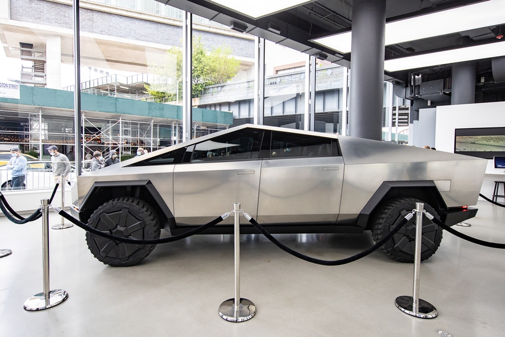
Anyway, the Korea Economic Daily article also mentioned that Tesla plans on unveiling the Tesla Cybertruck, which is expected to be equipped with HW 4.0 in late 2022, which suggests that HW 4.0 may not be available to use in Tesla's automotive vehicles until ~2023 at the earliest, especially since having HW 4.0 be compliant with ISO 26262 standards can be a very lengthy process, which I assume is the reason why Tesla's trying to start mass manufacturing of HW 4.0 by Q4 2021 at the earliest.

Considering that securing enough capacity for any process node probably requires companies to make plans a couple of years in advance, there's a possibility yields for Samsung's 7LPP process node probably weren't very good when Nvidia was in the process of securing process node capacity with Samsung, considering Nvidia originally planned on using Samsung's 7LPP process node for consumer Ampere GPUs, and especially with the process of being compliant with ISO 26262 standards being very lengthy. And speaking of process nodes, I think there's a possibility that Nvidia's waiting until Hot Chips 34 to announce which process node's used to fabricate the Orin family of SoCs.
 
Last edited:
I don't think Dojo D1 is the same as HW 4.0 since Dojo D1 has been described as a supercomputer, whereas HW 4.0's been described as a computer, as implied by HW 4.0's alternative name, FSD Computer 2. Also, Tesla mentioned that 2 x 3 Dojo D1 tiles in a tray can be combined with two trays in a computer cabinet, which sounds more like a datacentre configuration than SoCs equipped inside a vehicle. And I don't know if 2 x 3 Dojo D1 tiles in a tray that can be combined into two trays in a computer cabinet can fit inside an automotive vehicle.

Anyway, the Korea Economic Daily article also mentioned that Tesla plans on unveiling the Tesla Cybertruck, which is expected to be equipped with HW 4.0 in late 2022, which suggests that HW 4.0 may not be available to use in Tesla's automotive vehicles until ~2023 at the earliest, especially since having HW 4.0 be compliant with ISO 26262 standards can be a very lengthy process, which I assume is the reason why Tesla's trying to start mass manufacturing of HW 4.0 by Q4 2021 at the earliest.

Considering that securing enough capacity for any process node probably requires companies to make plans a couple of years in advance, there's a possibility yields for Samsung's 7LPP process node probably weren't very good when Nvidia was in the process of securing process node capacity with Samsung, considering Nvidia originally planned on using Samsung's 7LPP process node for consumer Ampere GPUs, and especially with the process of being compliant with ISO 26262 standards being very lengthy. And speaking of process nodes, I think there's a possibility that Nvidia's waiting until Hot Chips 34 to announce which process node's used to fabricate the Orin family of SoCs.

Thanks for the response and you bring to light a number of good points, all of these code names for silicon in development gets confusing to track at times. My main reasoning for bringing up the Samsung and Tesla venture is that most searches a month or so prior to that September article kind of made it seem like Tesla were leaning closer to going with TSMC for HW 4.0. The turn around from that article from when they hope to have it in production is a fairly quick turnaround unless TSMC were never really in consideration...
 
Thanks for the response and you bring to light a number of good points, all of these code names for silicon in development gets confusing to track at times. My main reasoning for bringing up the Samsung and Tesla venture is that most searches a month or so prior to that September article kind of made it seem like Tesla were leaning closer to going with TSMC for HW 4.0. The turn around from that article from when they hope to have it in production is a fairly quick turnaround unless TSMC were never really in consideration...
I think there's a possibility China Times has confused Dojo with HW 4.0. Ganesh Venkataramanan described Dojo's training tile as a integration of 25 known good D1 dies in a fan out wafer process. And based on the Ganesh Venkataramanan's description of Dojo's training tile, Dylan Patel from SemiAnalysis speculates Tesla is very likely using TSMC's Integrated Fan-Out System-on-Wafer (InFO_SoW) packaging for Dojo's training tile, which I think does suggest that Tesla's using TSMC's 7 nm** process node to fabricate D1 and package Dojo. I think there's a possibility that Tesla's indeed working with Broadcom to design Dojo as the rumour from China Times mentions, considering Google's said to have worked with Broadcom to design the Tensor Processing Unit (TPU). And going by AppleTrack's tracking of the accuracy of China Times, a good amount of rumours tend to be accurate, with some of the rumours tend to not be accurate.

And considering Tesla used Samsung's 14 nm** process node to fabricate FSD, or HW 3.0, there's a possibility that Tesla was planning to use Samsung's 7LPP process node to fabricate HW 4.0 for a very long time, if not from the very beginning.
 
0
I think it depends on if Nintendo's okay with a battery life range of 2.5 - 6.5 hours for the DLSS model*. Hypothetically, Nintendo could have kept the Nintendo Switch (2019)'s battery life range the same as the Nintendo Switch (2017), but increase the CPU, GPU, and RAM frequencies. However, Nintendo ultimately kept the Nintendo Switch (2019)'s CPU, GPU, and RAM frequencies the same, which resulted in a ~36.46% - 80% increase in battery life compared to the Nintendo Switch (2017). I think that might be an indication that Nintendo might not be okay with a battery life range of 2.5 - 6.5 hours.
Honestly, it was probably just a production cost consideration. While a smaller battery was required for the Lite model, keeping the same 16Wh battery from the OG Switch in the Mariko model meant they could continue getting volume discounts by maintaining those production orders, which they likely did because they had no use for the extra space that a smaller battery in the standard Switch would give them anyways.
So they get to continue reaping volume discounts on the 16Wh battery, while also getting more SoCs per wafer. The battery boost in the standard Switch likely just made it an absolute no-brainer to go that route, not purely because they wanted that battery boost to happen; it was good for production cost considerations AND benefitted the end consumer to boot.
That they even used that same battery part in the OLED model and opted to shrink other parts instead tells me it was far cheaper to keep the same battery at the same dimensions than to produce a new battery part.

TL;DR - I consider the bump in battery life to be a coincidental benefit to a production cost decision. If Dane gets better battery performance, it'll be due to engineering advances in battery density going down in price by the time they start fabrication of Dane hardware, not because they definitely want to hit a better number than what they had at Switch's launch. It'll be a nice-to-have.
 
Last edited:
Now that we are talking about batteries, I wonder if by 2030 we will have a hybrid, affordable battery that may be used in a Switch-like device? There are some commercially available already, but it'll be a long time before they can be in a gaming device I think. As for full graphene batteries... maybe by 2040, I doubt Nintendo will have abandoned the production of hardware by then even if the other 2 transitioned to full on subscription services.
 
0
I think it depends on if Nintendo's okay with a battery life range of 2.5 - 6.5 hours for the DLSS model*. Hypothetically, Nintendo could have kept the Nintendo Switch (2019)'s battery life range the same as the Nintendo Switch (2017), but increase the CPU, GPU, and RAM frequencies. However, Nintendo ultimately kept the Nintendo Switch (2019)'s CPU, GPU, and RAM frequencies the same, which resulted in a ~36.46% - 80% increase in battery life compared to the Nintendo Switch (2017). I think that might be an indication that Nintendo might not be okay with a battery life range of 2.5 - 6.5 hours.
I do think Nintendo thinks battery life is important, but who plays more than 2.5 hrs anyway on handheld straight? I hope Nintendo gets as high clocks as possible
for the initial release and then give it V2 battery life for the revision...
 
Last edited:
The battery life will determine what node will be used for the next SoC. Mariko's 4-5W power consumption would seem impossible with Orin NX performance on 8nm.

8 nm would imply either lower performance (4SM) with a lower transistor budget (80-120mm2) but able to consume as low as 4-5W in handheld mode and thus on a Lite model. Or they would use 8 nm for the hybrid model only with a larger transistor budget (120-180mm2) with NX performance and release RedboxDane/LiteDane 2 years later on 5 nm.

Either way, 8cx3 and G3x will be a good indication of what to expect from a 5nm chip intended for a gaming console. Moreover, the Razer dev platform has the particularity to use switch-like form factor as opposed to deck/aya/gpd that are targeting a 15W TDP in handheld mode.
there's nothing about 8nm that says they're limited to 4SM. they can do 6 or even 8SM at lower clocks
 
0
The battery life will determine what node will be used for the next SoC. Mariko's 4-5W power consumption would seem impossible with Orin NX performance on 8nm.
Why? It’s a hybrid, it isn’t meant to clock to the max in portable mode.
8 nm would imply either lower performance (4SM) with a lower transistor budget (80-120mm2) but able to consume as low as 4-5W in handheld mode and thus on a Lite model. Or they would use 8 nm for the hybrid model only with a larger transistor budget (120-180mm2) with NX performance and release RedboxDane/LiteDane 2 years later on 5 nm.
The device was gonna have a portable mode regardless though, with 4, 6 or even 8SMs so it wasn’t gonna clock higher.
Either way, 8cx3 and G3x will be a good indication of what to expect from a 5nm chip intended for a gaming console. Moreover, the Razer dev platform has the particularity to use switch-like form factor as opposed to deck/aya/gpd that are targeting a 15W TDP in handheld mode.
It has to actually get off the ground first for that to be a realistic prospect :p
 
0
I do think Nintendo thinks battery life is important, but who plays more than 2.5 hrs anyway on handheld straight? I hope Nintendo gets as high clocks as possible
for the initial release and then give it V2 battery life for the revision...
90% of the time when I play portal I am plugged in (or could easily be.)

I’d gladly sacrifice some battery life for increased performance. I’m sure that’s not the case for everyone but I feel it’s pretty easy to have a battery pack or an outlet around in most cases.
 
90% of the time when I play portal I am plugged in (or could easily be.)

I’d gladly sacrifice some battery life for increased performance. I’m sure that’s not the case for everyone but I feel it’s pretty easy to have a battery pack or an outlet around in most cases.
I think most people are willing to make that sacrifice within reason. Again, 38-40 million Switch owners were cool with the battery life the OG was hitting.

It is important to keep in mind, as well, that battery density has undoubtedly improved since 2016 when Switch's battery spec was decided. Nintendo managed to squeeze more life out of that same battery with an SoC revision while that 2016-engineered battery got easier and cheaper to manufacture. Whatever the battery pricing was when OG Switches ran off the production line for launch is likely around the price they'll not want to exceed, while also balancing things out to a similar rate of battery life to the 2017 launch at least.
 
For someone who is not very tech savy, could someone explain how much was actually know about Orin and Dane so far? We know Dane is in the Switch code and its rumoured it will run on Orin right? And from what we know Orin could be used for a device like the Switch?
 
I just hope they don't end up with a bandwidth bottleneck. Honestly if the current Switch was better in this department I think you'd find a decent output improvement without changing anything else cpu/gpu wise.
 
For someone who is not very tech savy, could someone explain how much was actually know about Orin and Dane so far? We know Dane is in the Switch code and its rumoured it will run on Orin right? And from what we know Orin could be used for a device like the Switch?
Dane is not in the switch code

here's the break down
 
I know that Nintendo's most likely to continue using Arm based SoCs for a very long time.

However, Imagination Technologies seems serious about filling the same niche Arm fills, except in the RISC-V ecosystem, with the announcement of the Catapult family of RISC-V CPUs.

So in a hypothetical scenario that Nintendo wants to migrate from Arm to RISC-V, Imagination Technologies is definitely an option for Nintendo, especially since Imagination Technologies also has a GPU IP. And another hypothetical advantage of working with Imagination Technologies in the future is that Nintendo won't be subject to US export regulations since all of the IPs from Imagination Technologies is based in the UK, which is the same reason why Huawei's allowed access to the Armv9 licence. And that's especially important if Nintendo wants to continue selling in China, which Nintendo most definitely wants to do, especially with Nintendo currently partnering with Tencent to sell Nintendo Switch units in China.
 
Last edited:
I know that Nintendo's most likely to continue using Arm based SoCs for a very long time.

However, Imagination Technologies seems serious about filling the same niche Arm fills, except in the RISC-V ecosystem, with the announcement of the Catapult family of RISC-V CPUs.

So in a hypothetical scenario that Nintendo wants to migrate from Arm to RISC-V, Imagination Technologies is definitely an option for Nintendo, especially since Imagination Technologies also has a GPU IP. And another hypothetical advantage of working with Imagination Technologies in the future is that Nintendo won't be subject to US export regulations since all of the IPs from Imagination Technologies is based in the UK, which is the same reason why Huawei's allowed access to the Armv9 licence. And that's especially important if Nintendo wants to continue selling in China, which Nintendo most definitely wants to do, especially with Nintendo currently partnering with Tencent to sell Nintendo Switch units in China.
I've always felt like Nintendo benefits a lot more working with nvidia as their GPU techs are scaled down from their desktop designs and benefit from nvidia's drivers and breakthroughs like DLSS. I feel like its what party made Switch so powerful at launch in 2017, given the Tegra X1 was already in a retail product prior to its launch and was rather mediocre as an android device without the benefit of more dedicated nvn apis Switch has access to.

Working with a purely mobile GPU company that doesn't have the software prowess of nvidia and having to build an API on their own wouldn't have as much value to them. It's why I feel the nvidia partnership is sticky for them.
 
Last edited:
0
One of Swi

I've always felt like Nintendo benefits a lot more working with nvidia as their GPU techs are scaled down from their desktop designs and benefit from nvidia's drivers and breakthroughs like DLSS. I feel like its what party made Switch so powerful at launch in 2017, given the Tegra X1 was already in a retail product prior to its launch and was rather mediocre as an android device without the benefit of more dedicated nvn apis Switch has access to.

Working with a purely mobile GPU company that doesn't have the software prowess of nvidia and having to build an API on their own wouldn't have as much value to them. It's why I feel the nvidia partnership is sticky for them.
Fully agree! We all like to focus on power, but the software/ hardware package that Nvidia is able to provide is unmatched in the mobile tech industry.
 
0
I know that Nintendo's most likely to continue using Arm based SoCs for a very long time.

However, Imagination Technologies seems serious about filling the same niche Arm fills, except in the RISC-V ecosystem, with the announcement of the Catapult family of RISC-V CPUs.

So in a hypothetical scenario that Nintendo wants to migrate from Arm to RISC-V, Imagination Technologies is definitely an option for Nintendo, especially since Imagination Technologies also has a GPU IP. And another hypothetical advantage of working with Imagination Technologies in the future is that Nintendo won't be subject to US export regulations since all of the IPs from Imagination Technologies is based in the UK, which is the same reason why Huawei's allowed access to the Armv9 licence. And that's especially important if Nintendo wants to continue selling in China, which Nintendo most definitely wants to do, especially with Nintendo currently partnering with Tencent to sell Nintendo Switch units in China.

I do wonder since the Arm/Nvidia merger are all but dead now, will Nvidia try to go after a company like SiFive in order to have their own in-house CPU designs. RISC-V is definitely making performance gains in comparison to current ARM and Intel chips and sounds flexible enough to meet the needs of HPC and be able to scale down to a Switch like gaming device in the future if Nvidia chose to go that way.(In reading into the company's history it seems that Intel themselves are very interested in SiFive as well)
 
I do wonder since the Arm/Nvidia merger are all but dead now, will Nvidia try to go after a company like SiFive in order to have their own in-house CPU designs. RISC-V is definitely making performance gains in comparison to current ARM and Intel chips and sounds flexible enough to meet the needs of HPC and be able to scale down to a Switch like gaming device in the future if Nvidia chose to go that way.(In reading into the company's history it seems that Intel themselves are very interested in SiFive as well)
NVIDIA already has an ARM architecture licence
 
I do wonder since the Arm/Nvidia merger are all but dead now, will Nvidia try to go after a company like SiFive in order to have their own in-house CPU designs. RISC-V is definitely making performance gains in comparison to current ARM and Intel chips and sounds flexible enough to meet the needs of HPC and be able to scale down to a Switch like gaming device in the future if Nvidia chose to go that way.(In reading into the company's history it seems that Intel themselves are very interested in SiFive as well)
ARM provides licenses that let you make fully custom cores (see: Apple) which I believe Nvidia already has.

Granted, I could definitely see Nvidia getting really petty and going all in on RISC-V, but it's not a legal requirement.
 
I've always felt like Nintendo benefits a lot more working with nvidia as their GPU techs are scaled down from their desktop designs and benefit from nvidia's drivers and breakthroughs like DLSS. I feel like its what party made Switch so powerful at launch in 2017, given the Tegra X1 was already in a retail product prior to its launch and was rather mediocre as an android device without the benefit of more dedicated nvn apis Switch has access to.

Working with a purely mobile GPU company that doesn't have the software prowess of nvidia and having to build an API on their own wouldn't have as much value to them. It's why I feel the nvidia partnership is sticky for them.
Before I start, I want to be very clear that I believe that Nintendo's going to continue working with Nvidia for a very long time for obvious reasons.

Also, I don't know if any company outside of Nintendo has been involved in the development of the Wii U's API, so I could be wrong when the Wii U's API's concerned. Anyway, I don't deny the fact that Imagination's software prowess won't be as good as Nvidia's software prowess; and I don't deny the fact that Nintendo would probably need to do more work on the API if Nintendo hypothetically decides to work with Imagination Technologies rather than continue working with Nvidia in the future. But saying that, I don't think Nintendo necessarily needs to develop an API completely from scratch, like with the Wii U, considering that Imagination Technologies mentions "full hardware and software support for heterogeneous SoCs using Imagination IP cores", and IMG CXT GPU does support APIs like Vulkan 1.2 + extensions, OpenGL ES 3.x/2.0/1.1 + extensions, and OpenCL 3.0. (Of course, I don't know if Imagination Technologies is bluffing here. And I don't know how extensively Imagination Technologies would work with Nintendo when developing an API.)

And one disadvantage with continuing to work with Nvidia is that Nintendo's subject to US export restrictions since Nvidia's tech is considered to be US technology by the US government since Nvidia's based in the US. And in the hypothetical scenario where the US government puts Tencent in the Entity list, Nintendo can no longer send products to Tencent to sell in China, unless Nintendo applies for a licence that would allow Nintendo to send products to Tencent to sell in China. (The US government did consider adding Tencent in the Entity list, but I believe that was scrapped.)

~

NVIDIA already has an ARM architecture licence
ARM provides licenses that let you make fully custom cores (see: Apple) which I believe Nvidia already has.

Granted, I could definitely see Nvidia getting really petty and going all in on RISC-V, but it's not a legal requirement.
I think NineTailSage is talking about a hypothetical scenario where Nvidia would want to acquire a chip designer in the likely scenario where Nvidia's attempt to acquire Arm is blocked, similar to how Qualcomm acquired Nuvia.
 
Last edited:
Before I start, I want to be very clear that I believe that Nintendo's going to continue working with Nvidia for a very long time for obvious reasons.

Also, I don't know if any company outside of Nintendo has been involved in the development of the Wii U's API, so I could be wrong when the Wii U's API's concerned. Anyway, I don't deny the fact that Imagination's software prowess won't be as good as Nvidia's software prowess; and I don't deny the fact that Nintendo would probably need to do more work on the API if Nintendo hypothetically decides to work with Imagination Technologies rather than continue working with Nvidia in the future. But saying that, I don't think Nintendo necessarily needs to develop an API completely from scratch, like with the Wii U, considering that Imagination Technologies mentions "full hardware and software support for heterogeneous SoCs using Imagination IP cores", and IMG CXT GPU does support APIs like Vulkan 1.2 + extensions, OpenGL ES 3.x/2.0/1.1 + extensions, and OpenCL 3.0. (Of course, I don't know if Imagination Technologies is bluffing here. And I don't know how extensive Imagination Technologies would work with Nintendo when developing an API.)

~


I think NineTailSage is talking about a hypothetical scenario where Nvidia would want to acquire a chip designer in the likely scenario where Nvidia's attempt to acquire Arm is blocked, similar to how Qualcomm acquired Nuvia.
You're right we don't know, but i'm just guessing a chip designiner targeting mobile phones will in general not be pushing their hardware in the way Nintendo requires. nVidia on the other hand has experience making drivers for their GPUs pushing them to their limits for gaming, which probably translated well to Nintendo's requirement for a close to the metal APIs being used on the Switch and as far as we can see, the performance improvement over the stock X1 in the SheildTVs running at higher clocks appear to be significant.

I'm am sure if there is a will to change vendors, there is a way, but there's always the risk then the tools don't end up being as good. From what I have read, working on the Switch has been pretty straightforward, i wonder if they can keep that if they switch vendors.
 
Last edited:
0
I think NineTailSage is talking about a hypothetical scenario where Nvidia would want to acquire a chip designer in the likely scenario where Nvidia's attempt to acquire Arm is blocked, similar to how Qualcomm acquired Nuvia.
Ah, I see.

Nvidia buying SiFive is probably less of a threat to RISC-V as an ISA than buying ARM would be, since I think SiFive doesn't actually own the core IP and the license allows for fork threats, but I have some doubts Nvidia doing Nvidia things would be healthy for what is supposed to be a very open architecture.

At the very least, this would probably indicate a "going all in on RISC-V" scenario, as that is SiFive's focus. The chances of that trickling down to Nintendo in that scenario are high, but it is probably a manageable switch with a good enough emulator on place.
 
ARM provides licenses that let you make fully custom cores (see: Apple) which I believe Nvidia already has.

Granted, I could definitely see Nvidia getting really petty and going all in on RISC-V, but it's not a legal requirement.

That's my guess is that Nvidia might be extremely petty over the merger going south...
 
0
I think Nvidia would just continue their custom design with Grace as a starting point
I don't think Grace is a custom Arm based CPU design since Nvidia mentioned using next-generation Arm Neoverse cores for Grace (Neoverse N2?).

~

I've always felt like Nintendo benefits a lot more working with nvidia as their GPU techs are scaled down from their desktop designs and benefit from nvidia's drivers and breakthroughs like DLSS. I feel like its what party made Switch so powerful at launch in 2017, given the Tegra X1 was already in a retail product prior to its launch and was rather mediocre as an android device without the benefit of more dedicated nvn apis Switch has access to.

Working with a purely mobile GPU company that doesn't have the software prowess of nvidia and having to build an API on their own wouldn't have as much value to them. It's why I feel the nvidia partnership is sticky for them.
I forgot to mention that one apparent advantage that Imagination Technologies has over Nvidia and AMD is in terms of ray tracing, considering Imagination Technologies claim that IMG CXT achieves level 4 in terms of ray tracing, which stands for "BVH processing with coherency sort in hardware". Nvidia on the other hand apparently achieves level 3 in terms of ray tracing, which stands for "BVH processing in hardware", and AMD apparently achieves level 2 in terms of ray tracing, which stands for "Ray/box and ray/triangle testers". Of course, I don't know how high Nintendo places ray tracing in terms of important hardware features.
 
Nvidia is actually level 4.
 

The conversation as a whole is interesting because the market needs continued competition in order to effect growth and prevent stagnation.

Another interesting article I came across (not sure how legitimate these claims are) Micro Magic has introduced what it claims is the world’s fastest 64-bit RISC-V core — a device it says outperforms the Apple M1 chip and Arm Cortex-A9. It's an interesting claim nonetheless because they also highlight how efficient their CPU core is in comparison to anything currently available...
 
0
Besides it being mentions as being level 4 (not 3), with respect to the RT hardware I think we should also take the possibility of using said hardware not just for RT but other uses as well, it’s raw compute that is accelerated by hardware.

While Nintendo is known to repurpose old technology, that doesn’t mean they can’t repurpose newer technology for a different use case.

I think that they can use it for dedicated Audio acceleration and have fancy audio (without having to pay a Dolby license).


I also wonder if they do include Maxwell SMs into the the mix, can they use those for acceleration of other features like audio if they don’t use the RT cores.
 
0
Nvidia is actually level 4.
DavidGraham on Beyond3D believes Nvidia's ray tracing implementation for Turing and Ampere GPUs is at level 3 since level 4 and level 5 apparently require more die space and more specialised hardware. And so far, I haven't found information that mentions that Nvidia's ray tracing implementation is at a level 4. (Perhaps Nvidia's ray tracing implementation is at a level 4 for Lovelace GPUs if what DavidGraham said is true?)

I'm curious about how IMG CXT compares to Orin and/or Dane when ray tracing implementation's concerned since Imagination Technologies mentions that IMG CXT has dedicated silicon dedicated to doing accelerated ray tracing in a more power efficient manner than what's possible in desktop GPUs.
Nvidia's patents mention bundling coherent rays together


And independent testing surmises that Nvidia is doing ray bundling to save performance


Who knows how Imagination would classify Dane. They can't even get their own product out
 
0
I just hope they don't end up with a bandwidth bottleneck. Honestly if the current Switch was better in this department I think you'd find a decent output improvement without changing anything else cpu/gpu wise.
I think we'll be fine, at least when compared to xbone and ps4 base. Nvidia architecture since Maxwell has been known to be really efficient with bandwidth, 64 bit LPDDR5 will put us a double the bandwidth of switch's 25.6 (51.2 GB/s) and that should will put us at xbone level at least. But there's a very good chance we'll get 88-102 GB/s bandwidth if we get 128 bit bus width., which I belive shouldn't be a problem when it comes head to head with PS4 games.

The absolute best case scenario is 102GB/s bandwidth with Orion NX's L2 and L34- 8mb cache tech which will help tremendously free and speed up bandwidth... Not to mention DLSS.
 
Please read this staff post before posting.

Furthermore, according to this follow-up post, all off-topic chat will be moderated.
Last edited:


Back
Top Bottom