I hope we can refine Thraktor's method to get these results for a wider range of GPU clocks and SM counts. That way, we could maybe have the full range of GPU options Nintendo had for this gen.
I finally was able to find where Thraktor got the number from.
oldpuck said:
My 27% number wasn't in reference to 5LPP, where we have to go by ARM data to get like-for-like. I have Ampere data from our compute farm that lets me compare Ampere on TSMC 7nm to Ampere on SEC 8nm. I was saying that a 30% power reduction would generally track with 5LPP being comparable to TSMC 7
First thing to note is that the tests were efficiency per cuda core, so the fact that the SM structure between A100 and GA10X is vastly different, isn't an issue. However A100 Cuda cores themselves are different, for one thing they do double precision VASTLY differently. A100 is 2:1, GA102 is 30:1, that means you need 2TFLOPs of fp32 on A100 to process 1TFLOPs fp64, however you need 30TFLOPs fp32 to process 1TFLOPs fp64 on RTX 3080. These cores are different, they are all clocked much higher than Drake, which is important for later, lets continue.
The comparison between TSMC 7nm and Samsung 5LPE exists, it was done by
Anandtech here (oldpuck and dakhil helped me source this stuff btw, thanks oldpuck, dakhil):
At lower performance levels, we noted that the 5LPE node doesn’t look to be any different than TSMC’s N7P node, as the A55 cores in the Snapdragon 888 performed and used up exactly the same amount of power as in the Snapdragon 865. At higher performance levels however, we’re seeing regressions
We also have the
Exynos 9820 vs the Exynos 9825, 8LPP vs 7LPP, even if you just pretend that these devices pull the same wattage from all other components and it was just the 9820 with 4100mah vs 9825 3500mah, the 9825 last 8% longer, while the 9820 has a battery 17% bigger. Ultimately this means that Samsung 7LPP is greater than 22% reduction of power (it is even better than this when taking into account the slightly higher clocks and larger screen).
Then going back to the
Anandtech link:
Generationally, Samsung seems to have been able to greatly reduce voltages this generation. On the Cortex-A55 cores, the cores now only require 800mV at 2GHz whilst the Exynos 990 last year in our review unit they required over 1050mV.
We see that the move from 7LPP to 5LPP results in a reduction of power consumption by ~24%.
There is a reduction of
5% from 5LPE to 5LPP.
The reduction from 8LPP to 7LPP is ~25%, then the reduction from 7LPP to 5LPE is ~24%, meaning Orin on 5LPP would consume around ~54% at the same frequencies.
We can check to see how roughly correct this all is by checking
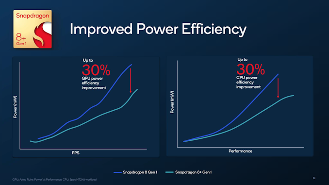
8 Gen 1 (Samsung 5LPP/4LPX) vs 8 Gen 1+ (TSMC 4nm)
Officially, Qualcomm is claiming a 30% improvement in both GPU and CPU power efficiency. Though as mentioned before, this is at iso-frequency and doesn’t take into account the higher peak clockspeeds of the 8+ Gen 1. Consequently, the real-world power savings aren’t going to be quite as great on a peak-to-peak basis, but according to Qualcomm the power savings are still significant. Overall, the company is touting a 15% reduction in SoC power usage under “practical usage patterns” versus the original 8 Gen 1, which in turn should lead to improved battery lifetimes in handsets that adopt the new SoC.
What the picture above shows is that the 30% reduction in power consumption from Samsung 5LPP/4LPX to TSMC 4nm is at the higher frequencies, pushing upwards of twice the frequency of Drake's SoC, where it would be in the neighborhood of ~10% to ~15%.
But TSMC 4nm isn't TSMC 4N, TSMC 4N is TSMC 5nm (thank Nvidia for that), so what is the power reduction from TSMC 5nm to TSMC 4nm?
22%.
This number is likely also the high end frequency, and likely is smaller than Samsung 5LPP to TSMC 4nm, but obviously not by very much.
All the above info leads to this. An Orin chart with these realistic clocks for "Switch 2"s handheld mode:
Orin (High load) CPU: 1881MHz, (High load) GPU: 624.75MHz
Samsung
8LPP - ~13.1w
7LPP - ~9.8w
5LPP - ~7w
TSMC
7nm - ~7.4w
5nm - ~6.3w
4nm - ~5w
Drake would offer lower power consumptions than this chart, possibly by as much as 10%, because it uses some power saving features from Ada, and because it has less cache and other differences to Orin.
Here is some final things to note, when Qualcomm moved from Samsung 5LPP to TSMC 4nm on the 8 gen 1(+), they increased the GPU from 618MHz to 680MHz, a 10% increase, but maybe much more interesting, the GPU is a little over 2TFLOPs, and unless it is vastly different in efficiency, that means it's passively cooled and finds it's power curve around 600MHz on 5LPP, Drake's architecture is obviously different, so it will be different in power draw per flop, however this likely means Drake's clock IF 5LPP is going to be around 600MHz, but one thing interesting to note about the current Switch, is that it runs it's portable clock as high as 460MHz, which was done in botw, seemingly since launch because battery tests never changed when newer models came out, this is higher than TX1's known power curve, which could mean they are looking at the 660MHz clock (if it is the target) in much the same way as the 460MHz clock.
The difference between 460MHz in portable and 768MHz in docked (67%) is very similar to these found clocks, 660MHz in portable and 1125MHz docked (70%). In fact, it's even slightly more aggressive than these new clocks would be.
As much work as Thraktor put into his post, I do think that he was working with inaccurate data, it's a lot of great data, and through, but just it's square shaped, and the hole is round.