
D
Deleted member 2
Guest
Not true, because I couldn't functionally play it on my Switch.So was the first version of Ark I guess.
If you argue that "you couldn't functionally play Doom on your Switch", well, you'd be wrong.
Not true, because I couldn't functionally play it on my Switch.So was the first version of Ark I guess.
It wouldn’t be that small of an increase unless you believe that the rest will actually decrease in sizeI just want to mention that I don't think die size is much of a relevant consideration when we talk about which process node nintendo will choose for the drake. They could literally double the die size from the Erista and that'd only translate to an additional 5mm increase (or 1/5th of an inch for the americans) in chasis size in each direction. This might be a consideration for smaller form factors such as phones, but for the switch that'd only correspond to a 3% increase in length and 5% increase in height. A larger die would also benefit from increases in passive cooling so there also is much more to the story with regards to heat. I imagine the only major consideration for process node selection is going to be power consumption and the associated battery life implications.


I'll gladly carry the torch on that aspect. Not just out of personal preference but because there is no evidence to support a larger chassis. They knew, years ago, what they would be aiming for with this. They wouldn't have been blindsighted by the size of the SOC. They also know that the market is sensitive to aesthetics and portability, a failure they will not repeat from the Wii U. They have over a hundred million users they want to convert and every chance to make their new device a drop in replacement.I spent every ounce of effort to hold my tongue
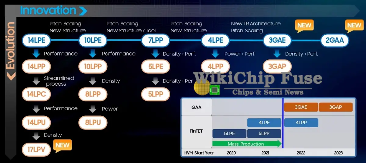
So there are basically 3 generations worth of suspects here.For my simple mind, can someone make a list, from best to worst, of the process nodes that Drake could be on? My mind reels with all the 4N and N4 and Samsung this and TSMC that… I’m assuming the list would start with 3nm TSMC being best (but unlikely), and 8nm Samsung being worst, right? Where do all the 4Ns and N4s fit between there?
)
Happy Mar10 Day?
There won't be an onboard tx1 +.
It would limit their options somewhat around having some types of middle ground modes, but there will only be barriers to full upgrade patches if they intentionally construct them.Question regarding backwards compatibility, if Nintendo went the route of including a TX1 in the Switch 2 so when you play a Switch game the system reverts into ‘OG Switch mode’ would that then mean any type of boost mode or upgrade patches for Switch games would be impossible?
There are more possible nodes than you can shake a stick at, but most of them are just slightly tweaked versions of each other.For my simple mind, can someone make a list, from best to worst, of the process nodes that Drake could be on? My mind reels with all the 4N and N4 and Samsung this and TSMC that… I’m assuming the list would start with 3nm TSMC being best (but unlikely), and 8nm Samsung being worst, right? Where do all the 4Ns and N4s fit between there?
And Nvidia mentioned during GTC 2021 (November 2021) datacentre products (BlueField-3, Quantum-2, ConnectX-7) that were fabricated using TSMC's 7N process node and were sampling at around late 2021 to early 2022.The evidence of Nvidia having some supply here is the A100.
It wouldn’t be that small of an increase unless you believe that the rest will actually decrease in size
This is the TX1 and the TX1+
If the chip is 50% bigger, the substrate it sits on will also be bigger
And if the substrate is bigger, the board is bigger, and if the board is bigger then the device will also be bigger in every direction (well, except depth)
Though the length would be ok, the height wouldn’t really as that would end up breaking the Joycon compatibility, if they care for that.
So there are basically 3 generations worth of suspects here.
Best: TSMC 4N, which is a Nvidia-specific variant within TSMC's N5 family which is part of the 5 nm generation. We know that Nvidia has secured some supply of this node because of the Lovelace/RTX 40 series cards.
Middle: TSMC N6, that's a refinement/variant of TSMC's N7, which is part of the 7 nm generation (which is one generation behind 5 nm). The evidence of Nvidia having some supply here is the A100.
Worst: Samsung 8LPP, that's a refinement of Samsung's 10 nm node family (and one generation behind 7 nm, or two behind 5 nm). The RTX 30 cards as well as Orin are on this node.
(gee, why do I have to say which node is part of which generation despite it seeming obvious? Because of Samsung's 5LPE. That node is a refinement of Samsung's 7 nm node, so it's not a 5 nm generation process
Thanks! It does make sense that where Nvidia is involved, it’s more likely than others to be a candidate for Drake. I just gotta keep fingers crossed for TSMC 5nm.There are more possible nodes than you can shake a stick at, but most of them are just slightly tweaked versions of each other.
Samsung 8nm: the default. Orin and RTX 30’s node. It’s a long lived node, it’ll be around for a while, getting cheaper.
Samsung 7LPP/6LPP: this is highly unlikely, unless Samsung gave Nvidia a crazy deal. A “true” 7nm node, the 6nm version is just a variation.
TSMC 7nm: the wild card. Nvidia’s data center Ampere chip is here. TSMC is trying to retire it for “6nm” which is really the 7nm with a few extra bells and whistles.
Samsung 5nm LPE, 5nm LPP, 4nm LPE: Samsung’s 5nm nodes. LPE means “low power early” and “LPP” is “low power plus”. There is improvement across these things but they should be seen as fundamentally the same technology.
TSMC 5N, N5, N4: TSMC’s 5nm nodes. 5N is Nvidia’s modified version for their RTX 40 chips. Also a long lived node, by design, but currently a near-bleeding edge node.
3nm: again both Samsung and TSMC are working on something here and Nvidia is heavily rumored to be using it for RTX 50, though Nvidia is complaining about shouldering costs for developing immature nodes and at least one person has claimed on my presence that they plan on staying on 5nm
Short of something deeply wild happening, I think places where Nvidia has products are the only viable spots.

Middle: TSMC N6, that's a refinement/variant of TSMC's N7, which is part of the 7 nm generation (which is one generation behind 5 nm). The evidence of Nvidia having some supply here is the A100.
To me, this is the sleeper hit. Both Ampere and ARM already build on it, there are no capacity or demand questions, unlike 5nm, and the density over 8nm is 80%. At that point, even the pessimistic numbers get us to modest clock increases and modest improvement over launch Switch battery life. It's cheap and it requires a relatively small amount of invested work.And Nvidia mentioned during GTC 2021 (November 2021) datacentre products (BlueField-3, Quantum-2, ConnectX-7) that were fabricated using TSMC's 7N process node and were sampling at around late 2021 to early 2022.
You mentioned cheap.To me, this is the sleeper hit. Both Ampere and ARM already build on it, there are no capacity or demand questions, unlike 5nm, and the density over 8nm is 80%. At that point, even the pessimistic numbers get us to modest clock increases and modest improvement over launch Switch battery life. It's cheap and it requires a relatively small amount of invested work.
Not necessarily. You know that the Mariko switch can be overclocked further right? And the TX1 CPU is somehow compatible to the A78 CPU. In that sense, Nintendo can just include the GPU part of TX1, increase the clock of the GPU, and use the Drake CPU to give "boost" performance.Question regarding backwards compatibility, if Nintendo went the route of including a TX1 in the Switch 2 so when you play a Switch game the system reverts into ‘OG Switch mode’ would that then mean any type of boost mode or upgrade patches for Switch games would be impossible?
@ the boldedBesides the SoC, the Switch has quite a few controllers on the board, power, peripherals, memory, display, wi-fi, etc. All of those may require quite a bit of circuitry and boilerplate. These are just guesses, I'm way out of my area here.
Could it be that Drake, being custom-made, would integrate some of those controllers, freeing some real estate on the board?
It would also simplify production and sourcing quite a bit, I believe.
The quality of the port matters a lot on Switch. Panic Button's efforts are okay, but meager when compared to some other developers who work much closer to the metal, such as Feral Interactive and Iron Galaxy.
Not true, because I couldn't functionally play it on my Switch.
If you argue that "you couldn't functionally play Doom on your Switch", well, you'd be wrong.
I do not think that Doom is a great port.
Depressing to think Nintendo would use 7nm tsmc, 3+4 years after Sony/Ms.To me, this is the sleeper hit. Both Ampere and ARM already build on it, there are no capacity or demand questions, unlike 5nm, and the density over 8nm is 80%. At that point, even the pessimistic numbers get us to modest clock increases and modest improvement over launch Switch battery life. It's cheap and it requires a relatively small amount of invested work.
That's one of those "wanting more only because it was compared to something else". 7nm/6nm would be fine and would give us the clocks and performance we are expecting with good battery life. Anything more is just a bonusDepressing to think Nintendo would use 7nm tsmc, 3+4 years after Sony/Ms.
And Nvidia mentioned during GTC 2021 (November 2021) datacentre products (BlueField-3, Quantum-2, ConnectX-7) that were fabricated using TSMC's 7N process node and were sampling at around late 2021 to early 2022.
Imagine if we get to the beginning of March/April and it's just like it is now.....silence....
This isn't what happened though. Just a few days after that post the leakers said it wasn't happening any time soon. The peaceful silence we're in now is very different from the mounting silence then.Ayoooo
It wasn't supposed to be a gotcha or anythingThis isn't what happened though. Just a few days after that post the leakers said it wasn't happening any time soon. The peaceful silence we're in now is very different from the mounting silence then.
So, that all said, single core Geekbench 5 figures for existing consoles should be:
Switch - A57 @1GHz - 140
PS4 - Jaguar @1.6GHz - 200
XBO - Jaguar @1.75GHz - 219
PS5 - Zen 2 @3.5GHz - 873
Hypothetical numbers for a new Switch with A78 cores at different clock speeds would then be:
A78 @1.2GHz - 390
A78 @1.6GHz - 520
A78 @2.0GHz - 650
I'd say 2GHz is unlikely, and only really plausible with 4 cores, but it gives you an idea of where the range of single-core performance is. Even with half as many cores, the new Switch could comfortably outperform the last gen consoles on the CPU front, and my "best case scenario" of 6x A78 @1.6GHz (with a couple of A55s for the OS), would outperform them by over a factor of 2. Of course there's still a big gap to the PS5/XBSX, but if T239 being base on Orin means using A78 cores, then there's definitely scope for a very big CPU upgrade on the new model.
That's one of those "wanting more only because it was compared to something else". 7nm/6nm would be fine and would give us the clocks and performance we are expecting with good battery life. Anything more is just a bonus
Even on 8nm, it is hard to determine anything because there is no test on a SoC without the automotive features. We can’t know the extent to which they contribute to the heat, or battery and power consumption. That’s why I found the Orin tools to be deeply flawed, and why I felt they shouldn’t be taken as any kind of indicator of performance capacity when they were posted on here.No, there is an expectation by many that docked mode will offer 3Tflop of performance, but again, this requires a clock speed north of 1Ghz. I do not believe Drake at 8nm achieve this and fit within the power/thermal constraints of the Switch form factor.
you have to remember that Steam Deck is hobbled by a lot of inefficiencies: translation layers, non-native games, clocks being usage limited rather than power limited, etc. how much can power consumption be clawed back by fixing those? that's pretty impossible to really tell, but I would think that Drake would be much better on battery than the SDWould Nintendo really be able to get to a Switch 1 level of electricity consumption at 7nm?
Nintendo would want something that consumes way less electricity than the Steam Deck, but if it's on the same node as the Steam Deck then wouldn't it have to be significantly less powerful than the Steam Deck?
I'm just not seeing where the electricity savings are going to be coming from if Nintendo can't go with a smaller node.
GDC hasn't happened yetAyoooo
x86 vs ARM goes a waysyou have to remember that Steam Deck is hobbled by a lot of inefficiencies: translation layers, non-native games, clocks being usage limited rather than power limited, etc. how much can power consumption be clawed back by fixing those? that's pretty impossible to really tell, but I would think that Drake would be much better on battery than the SD
GDC hasn't happened yet
there was one instance where x86 matched and beat ARM at low end performance per watt, but it took ditching legacy for itx86 vs ARM goes a ways
Could be Samsung 5nm if this holds true. It would have been obvious that 8nm was too big for 12SMs when they were doing simulations. If they had committed to Samsung for Drake, Samsung 5nm would have been a viable option for a processor being designed in 2020.
Nintendo uses a CPU architecture, ARM, which is mainly used for mobile, where performance per watt is of utmost importance.Would Nintendo really be able to get to a Switch 1 level of electricity consumption at 7nm?
Nintendo would want something that consumes way less electricity than the Steam Deck, but if it's on the same node as the Steam Deck then wouldn't it have to be significantly less powerful than the Steam Deck?
I'm just not seeing where the electricity savings are going to be coming from if Nintendo can't go with a smaller node.
do you have an article on what was cut? I've often wondered if Microsoft ever considered relegating legacy Windows apps to a subsystem and telling AMD and Intel to update x86 to gain efficiency.there was one instance where x86 matched and beat ARM at low end performance per watt, but it took ditching legacy for it
oh? I hadn’t read this. neat.there was one instance where x86 matched and beat ARM at low end performance per watt, but it took ditching legacy for it
90% if it is just that. I’ve seen multiple videos poke up on YouTube in wake of @NintendoPrime’s that all quote this thread. None attribute it, but the phrasing keeps being the same.We've had the most Switch 2 activity since last year's leaks. I do wonder if it's just all people digging up the same stuff after the unverified Pokemon leak.
I think it's going to be the chip in the Nvidia leak, period.By the by, I'm probably a bit out of the loop, but I was wondering what the thing is with the Drake chip and whether it is solidly Ampere or if there are next-gen (Lovelace) features that we have been able to divine from the leak. Can someone help me understand this?
edit: Considering Ampere is on 8nm and we are looking at a potential move to a different node for Drake, that could also be some reason to suspect they might have Ada-fied the chip in the process, right (what do you think)?
do you have an article on what was cut? I've often wondered if Microsoft ever considered relegating legacy Windows apps to a subsystem and telling AMD and Intel to update x86 to gain efficiency.
there was an article a long time ago that detailed it that I can't find anymore. but I did find a review of a product showing Atom matching ARM at the time (and sometimes outperforming it in performance per watt). unfortunately, Atom didn't progress much further, being relegated to servers. Intel's efficiency cores take up the mantle, but ARM made big strides in the mean timeoh? I hadn’t read this. neat.
the chip is straight up Ampere. whatever changes made to it doesn't make it Lovelace because it doesn't have much of Lovelace's changes. they don't need to turn it into Lovelace just to get it onto a different nodeBy the by, I'm probably a bit out of the loop, but I was wondering what the thing is with the Drake chip and whether it is solidly Ampere or if there are next-gen (Lovelace) features that we have been able to divine from the leak. Can someone help me understand this?
edit: Considering Ampere is on 8nm Samsung/7nm TSMC and we are looking at a potential move to a different node for Drake, that could also be some reason to suspect they might have Ada-fied the chip in the process, right (what do you think)?