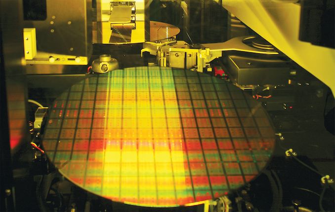
Thank you! Alright then. According to sources, the A12X has a die size of 122 m2 slightly bigger than 118m2 of the Switch Soc. Also, it should have a power draw of 15W according one of the sources I found (although this could not be corroborated by others) and by the time Dane launches, five years would have passed since the launch of the A12X.
So reasonably, before even touching questions such as costs and such, can we assume that Dane can compete with the A12X? If yes, it would be outstanding because we would be having the capability of a Xbox One S in the Switch Form factor. I hope that would be enough power for the devs as well.
No, sadly. Couple caveats to consider.
A12X was on the 7nm process at the time, Dane will be on 8N, which is supposed to be an improved version of 8LP(x). Node wise, it is already outclassed in logic.
CPU that the A12X has is clocked pretty high, and it curbstomps the Dane model CPU, it being 150% the multi-core performance that the Dane model would ever be. Unless Nintendo goes ballsy and clocks it pretty high, or just high enough to at least trade decent blows with the A12X. Single core score? Forget it. Though, this doesn’t really matter to be honest on a game console since they are always doing multi-threaded applications anyway. Single core matters more for phone things
GPU-wise, well this part I do expect it to be pretty competitive, but keep note its on a lesser node (presumably). What the iPad does is on a more efficient process, and does so at 15 watts
portably while the switch would not be using 15W in portable, likely around half of that. But it doesn’t matter since the GPUs in both are better than the GPU in the XB1 on paper specs.
The Dane will likely use a 4310mAh battery, while the iPad can use something like twice of this right? It’s less constrained by the power draw and can power higher yet still manage the battery life of the Mariko unit on the longer end.
HOWEVER! A couple points of contention, the iPad is not meant
for long gaming sessions unlike the Dane model. It has no active cooling, GPU being better on paper does not mean it’s better in real life performance, the thing can throttle down, though mobile devices have gotten pretty good with this regard.
Dane will be at a unique place, it will be more modern yet old at the same time and have a prettty heavy lean on the GPU side with ML hardware that allows it to push well above us weight.
Nintendo can possibly have a denser battery for the same size, like in the Samsung phones, that allows them to have a long battery life, slightly higher clocks which makes it more performant
before the docked mode boost.
Current mariko aims to draw only 6-7W I think, Erista drew like 9-11W or so portably. iPad draws 15W to perform its tasks (if I understood what you said correctly) at peak performance, but likely clocks down for energy saving reasons. Dane doesn’t need to do that clock switching, it’s a constant device.
It’s why I do hope they lean more onto the CPU being clocked modestly well at the sake of the GPU speeds. Should tide them over until the next platform rears it’s ugly head and we have the 7th speculation thread
")
A main takeaway is that this leans more into Apples to Oranges comparison.