That's a fair point regarding manufacturing process, and looking into it Samsung did announce they were working on an
automotive-grade 8nm process a couple of years ago. I'd still say with density pretty much identical to their 8N process, it's probably very close to standard 8N.
Regarding clock speeds, I don't think that's a process issue, I think it's just the reality of using a really big chip within the power/thermal limitations of the Jetson AGX form factor they've chosen (which is carried over from Xavier). They're limited to 50W for the full board, which means they're simply not going to be able to run a 460mm2 chip at full clocks. Consider that the GA104, which is a smaller die, consumes well over 200W when running at full clocks. The Drive AGX Orin doesn't seem to have the same limitation, as it advertises 254 TOPS (rather than 200), which would suggest a GPU clock as high as 1.5GHz (assuming the DLA clocks don't change much).
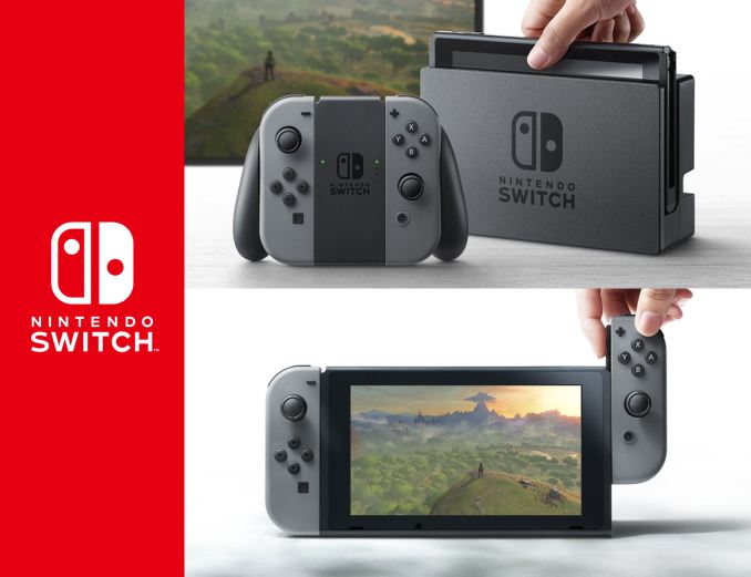
I actually wouldn't be surprised to see a Dane in the next Switch running higher clocks than Jetson Orin, perhaps up to about 1.2GHz docked, simply because with a smaller die and smaller GPU it'll have the capacity to.
I don't know what you mean by "unknown numbers" or what Xavier has to do with it, but here's my point: The TX1 was used in the original Switch and is about 121mm2 in size. I don't think it's reasonable to expect that their new chip for the next Switch (Dane) will be substantially bigger than that. We know from die shots of TX1 that Nvidia could spend 12mm2 of that 121mm2 on SMs. We also have a reliable source telling us that Dane is very similar in architecture to Orin, and we now know that an Orin SM takes up about 4.4mm2 of die space each (and that's the old Orin, they may be larger on the new 21b transistor Orin).
I'm saying that Nvidia might be able to squeeze 4 Orin SMs onto Dane, which would take up 17.6mm2, almost a 50% increase over TX1, and even then they're going to have to find that space somewhere else on the die. When people are saying they expect something like the Orin NX GPU for Dane, they're talking about
tripling the die area of SMs over TX1, which I think is unrealistic unless you expect a significantly larger die, which is just not something I expect.
Nintendo account for more of Nvidia's revenue than the entire automotive industry. The amount they'd lose by producing tens of millions of dies at twice the size they need to be would absolutely dwarf the R&D costs of using a different GPU configuration (which hey, they're going to have to do anyway, because they're clearly not using full Orin).
Note I said maybe some A55s. I'm not ruling out a full A78 setup, but I'm also not ruling out a couple of A55s. It could be two A55s, which should be sufficient to run Switch's OS, would take up less die space and less power than an A78 core, and would allow the system to run much more efficiently in low-power states (eg sleep mode).
Orin NX isn't Orin S.
You can see from Nvidia's photos that the die size of the Orin AGX and Orin NX chips is identical, so it's clearly a binned full Orin die.