• Hey everyone, staff have documented a list of banned content and subject matter that we feel are not consistent with site values, and don't make sense to host discussion of on Famiboards. This list (and the relevant reasoning per item) is viewable here.
  • Do you have audio editing experience and want to help out with the Famiboards Discussion Club Podcast? If so, we're looking for help and would love to have you on the team! Just let us know in the Podcast Thread if you are interested!

StarTopic Future Nintendo Hardware & Technology Speculation & Discussion |ST| (Read the staff posts before commenting!)

Intel, AMD, ARM, TSMC, and Samsung all support 'Chiplets' for future processor design

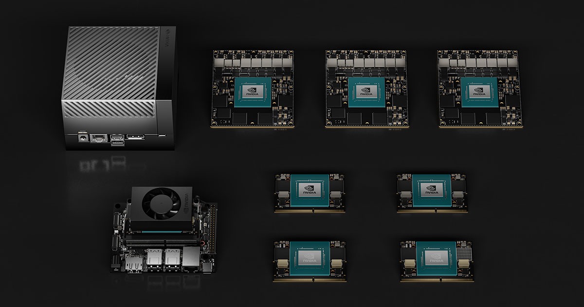
Intel, AMD, ARM, Samsung, Qualcomm, and TSMC, have come together to form a common and open standard for "Chiplets". A much smaller version of processors, chiplets have witnessed a massive growth in design, development, and adoption in the last few years. The Universal Chiplet Interconnect Express (UCIe), intends to standardize die-to-die interconnects for chipset designs with an open-source approach.

All the three leading-edge foundries, and dominant manufacturers of silicon wafers, have come together to announce that they are forming a new and open standard for chiplet interconnects. The UCIe hopes to simplify and standardize die-to-die connections in hardware and software. Eventually, such an approach could help designers and manufacturers of chips, CPUs, chipsets, and SoCs to easily and efficiently "mix and match" chiplets from different companies and create custom solutions.

Chiplets are essentially tiny blocks of integrated circuits. They are smaller than a traditional, monolithic CPU, and generally perform fewer tasks. Chiplets often lighten the load of the central processing cores. Interestingly, CPUs themselves can be designed as chiplets. In fact, Intel, ARM, and AMD are currently leading the development of processors which contain multiple chiplets. These new generations of CPUs have some performance cores and some efficiency cores. Other chiplets that are part of the package, include the integrated GPU, NPU, and perhaps even RAM and internal storage.

This seems pretty interesting and I wonder if future consoles will use this design as this seems similar to the normal setups.
 
Could T239 be used in data centres to enable cloud gaming the same way Xbox guts are used for Xcloud?

The proposition would be to enable 4k res in the current Switch library for NSO subscribers.

To go further, it could even be a Switch service that NSO subscribers could use on smart devices to play Nintendo gamss.
 
Could T239 be used in data centres to enable cloud gaming the same way Xbox guts are used for Xcloud?

The proposition would be to enable 4k gaming for NSO subscribers.

To go further, it could even be a Switch service that NSO subscribers could use on smart devices to play Nintendo gamss.
I think this would require Nintendo to make their own data centers around the world and that’s not cheap at all to build and maintain.

They could just utilize the NV cloud infrastructure or Amazon Web Services.
 
0
Well the reason for wanting a large die with 12 SMs may have to do with the fact that the amount of RT cores and tensor cores are tied to SM count. If they want this thing to have significant raytracing or AI/DLSS capabilities they might need more SMs to get them more of those dedicated cores.

As for them disabling SMs in portable mode, this would necessitate disabling those corresponding RT and tensor cores too, right? Couldn't that cause logic issues if they're using tensor cores for anything else besides DLSS, which is something you yourself have speculated on?
RT requirements should scale linearly with resolution, so that one shouldn't be a problem. Or, more specifically, the side of RT that's performed by RT cores on the GPU (such as BVH traversal and triangle intersection testing) should scale linearly with resolution. BVH generation doesn't scale with resolution, but that's typically handled on the CPU.

For tensor cores, any graphics applications will scale with resolution, which includes DLSS, but also a lot of potential interesting stuff like using it for non-realistic rendering (similar to style transfer). There are definitely potential non-graphical uses, which won't scale with resolution, but these fall into the same category as any other GPU compute, so wouldn't really be much different to the current Switch. They'd also be in the same scenario if they were just changing clocks. I'm also not saying that they'll have a precise 4x difference in performance, they could skew towards a bit more performance on the portable side to cover GPU compute use.
Hmmm I'm unsure I understand the latter part. I thought tensor cores had some unique coding to help handle AI tasks specifically. If you're using 48 tensor cores while playing Nintendogs in docked mode, and then you undock it which signals the GPU to cut off access to 24 of those cores, couldn't that interrupt specific AI related logic? Wouldn't that be kind of equivalent to dropping CPU clocks when you undock?

Or am I misunderstanding what tensor cores do exactly?
 
Intel, AMD, ARM, TSMC, and Samsung all support 'Chiplets' for future processor design


This seems pretty interesting and I wonder if future consoles will use this design as this seems similar to the normal setups.
Gaming tends to not like chiplets very much due to potential latency penalties, but at some point the benefits may outweigh the costs. At the very least, I'd expect Sony and Microsoft, with their much bigger chips, to adopt this before Nintendo does.
 
0
So what will the new OP header read like?

Future Nintendo Hardware & Technology Speculation and Discussion [ST] "You used to call me on my Samsung, ever since I left TSMC..."
 
So what will the new OP header read like?

Future Nintendo Hardware & Technology Speculation and Discussion [ST] "You used to call me on my Samsung, ever since I left TSMC..."
I like "You Drake Me a Believer"
 
Hmmm I'm unsure I understand the latter part. I thought tensor cores had some unique coding to help handle AI tasks specifically. If you're using 48 tensor cores while playing Nintendogs in docked mode, and then you undock it which signals the GPU to cut off access to 24 of those cores, couldn't that interrupt specific AI related logic? Wouldn't that be kind of equivalent to dropping CPU clocks when you undock?

Or am I misunderstanding what tensor cores do exactly?
Tensor cores are to AI what GPUs are to graphics.

Processors/GPUs/Tensor cores all fundamentally just Do Math. GPUs are designed to be really really good at the math you want to do to generate graphics. But it's also usable for other kinds of problems that use that same kind of math. Turns out AI was one of those problems, lots of people were using GPUs to do AI, which eventually lead to Nvidia building a way to accelerate just that math - the Tensor core.

If you turn off some of those cores, you are absolutely right, you will interrupt running tasks. There are just ways of handling that. One strategy is to turn off access to the cores before you power them down, letting running tasks have a short window to complete before they get cut off. On a 60fps game, the engine only has less than 17 milliseconds to complete all the tasks it has to draw the screen if it doesn't want to drop frames, so you don't have to keep them powered on long.

This isn't the only strategy - a game (generally) doesn't care directly how many cores their are, it hides that behind a sort of pool where it farms stuff out to what's available. So if half the cores power down, it has half the cores to farm stuff out too. If it knows it's undocked, and downscales the amount of work it is doing in total - for example, by lowering the resolution to match the smaller screen - you can keep the newer, smaller number of cores from getting overloaded.
 
0
Hidden content is only available for registered users. Sharing it outside of Famiboards is subject to moderation.
Thanks for the writeup. I have to apologize for the piecemeal nature of the info, as I did find out afterwards that the values are in units of giga-ops per second per SM at 1 GHz, which you already figured out. And there was another place that explicitly stated GA10F, like the rest of Ampere, has 128 FFMA32 units (aka CUDA cores, evidently) per SM. So the topline math all checks out.

@Ghostsonplanets also said that 1 GHz is the maximum clock for Orin, so if that's also true of Drake, then your calculations represent the theoretical maximum performance of GA10B/GA10F.
 
Last edited:
Hidden content is only available for registered users. Sharing it outside of Famiboards is subject to moderation.

Well, that does introduce the question of if it can run 4K DLSS or not with the number of TOPs here.
3TFLOPs of Drake likely will match up to the PS4 Pro or beat it outright because how much better the Drake uArch is versus Polaris.

But DLSS's cost scales mostly off the outut res right?

So if they are targeting a 4K output, it would require more TOPs (for 60fps)
 
Last edited:
So @LiC shared the following code snippet with @ReddDreadtheLead who shared it with me, and there was some confusion over exactly what it is, so I figured I'd share it in the thread with an explanation, as it provides some more details on expected performance. I should emphasise that I haven't seen any of the code around this, so I'm just inferring from the snippet below, but I think it's relatively self-explanatory, so I'm pretty confident in my deductions.
Hidden content is only available for registered users. Sharing it outside of Famiboards is subject to moderation.


That was quite a lot, so TLDR: This code indicates Drake has the same 128 CUDA cores per SM as desktop Ampere and Orin, and therefore has 1536 cores. It also indicates that the tensor cores on Drake operate at the same rate as desktop Ampere, not the double-rate tensor cores we see on Orin.
Thanks for the write up, but can I have one request? Is it possible to make it hidden for those who aren’t signed up :p

You too @oldpuck
 
Hmmm I'm unsure I understand the latter part. I thought tensor cores had some unique coding to help handle AI tasks specifically. If you're using 48 tensor cores while playing Nintendogs in docked mode, and then you undock it which signals the GPU to cut off access to 24 of those cores, couldn't that interrupt specific AI related logic? Wouldn't that be kind of equivalent to dropping CPU clocks when you undock?

Or am I misunderstanding what tensor cores do exactly?

You're not misunderstanding, it's just that migrating code to another SM before turning off cores is actually pretty straightforward. On both CPUs and GPUs there's a thread scheduler which swaps individual threads on individual cores, depending on priority, availability of data, etc. These thread schedulers can also migrate threads from one core to another (it's basically the same as switching from one thread to another, but when it switches back, it's on another core), and it's pretty standard on CPUs, the relevant example here being in the mobile space where threads are swapped back and forth between high-performance cores and high-efficiency cores to balance between performance and battery life. There's a minor performance impact from moving the registers to another core, repopulating the L1 cache, etc, but it's small enough not to be noticeable when it's done (very frequently) on smartphones, and in this case a user is docking or undocking the game, so is unlikely to notice any hitch in performance anyway.

Thanks for the writeup. I have to apologize for the piecemeal nature of the info, as I did find out afterwards that the values are in units of giga-ops per second per SM at 1 GHz, which you already figured out. And there was another place that explicitly stated GA10F, like the rest of Ampere, has 128 FFMA32 units (aka CUDA cores, evidently) per SM. So the topline math all checks out.

@Ghostsonplanets also said that 1 GHz is the maximum clock for Orin, so if that's also true of Drake, then your calculations represent the theoretical maximum performance of GA10B/GA10F.

Oops, it's actually ops per clock per SM (which happens to line up to giga-ops per second at 1GHz per SM, just because I chose a round 1GHz number). I've added a line to clarify that in the post.

Also, on Orin, it's the maximum supported clock for Orin's GPU on the Jetson AGX Orin board, but not for the Orin GPU in general. That hasn't been officially published, but Nvidia do state that Orin is capable of 254 TOPS in Drive AGX Orin, compared to 200 TOPS in Jetson AGX Orin, so there's very likely some increase in clock there. Given the same manufacturing process and largely similar GPU arch to desktop Ampere, I'd expect it can clock a lot higher than 1GHz, but that it's kept down to keep heat and power consumption in-check. That's also likely to be the main issue for Nintendo, rather than the technical max clock of the chip.
 
Based @Thraktor! Thanks for the write-up!
BTW, here's the link for Orin AGX specifications. As referenced by @LiC :
Max GPU Freq: 1GHz
edit: I see Thraktor. So it's probably the max frequency due to energy-consumption and heat concerns on AGX Orin. Thanks for the correction!
 
0
Thanks, done. @LiC and @Alovon11 , could you do the same (or just snip out the text of your quoted message)?
Hidden content is only available for registered users. Sharing it outside of Famiboards is subject to moderation.

That part for mine.
The Tensor Ops seems a bit low for Drake to do 4K DLSS at 60fps and if the system is a PS4-level system then it would be a bit of a complicated affair to utilize DLSS there unless if they have a DLA in it to up the TOPs back up, or if DLSS here uses NIS as part of it.
 
Last edited:
Quoted by: SiG
1
Wouldn’t that be a really small amount, especially with 12 SMs?

I’m betting we get multiple clock options in handheld for devs, like Switch currently has.
Might be at a higher precision, we don't have context here about clocks either, this might be in handheld clocks. /caught up to Thraktor's post, his reading is accurate and clears up the context issue, though clock is still unknown.
 
Last edited:
0
That part for mine.
The Tensor Ops seems a bit low for Drake to do 4K DLSS at 60fps and if the system is a PS4-level system then it would be a bit of a complicated affair to utilize DLSS there unless if they have a DLA in it to up the TOPs back up, or if DLSS here uses NIS as part of it.
I'm a bit confused...
What part of the Tensor Ops makes it hard to do 4k DLSS at 60fps? Isn't the DLSS portion now base-resolution-agnostic so they could perhaps reconstruct an image from 720p, even if the image quality isn't as good as native 4k (it would still be considered "good enough" for Nintendo)? Also isn't it dependent on what quality of DLSS they are aiming to achieve?
 
0
Well, that does introduce the question of if it can run 4K DLSS or not with the number of TOPs here.
3TFLOPs of Drake likely will match up to the PS4 Pro or beat it outright because how much better the Drake uArch is versus Polaris.

But DLSS's cost scales mostly off the outut res right?

So if they are targeting a 4K output, it would require more TOPs (for 60fps)

Yeah, DLSS is largely dependent on output res, but there is a bit of a difference depending on input res too (the higher the input res, the lower the performance requirement, at least by a bit).

I don't think DLSS to 4K/60 output is out of the realm of possibility at all, but I also don't think 4K/30 and 1440p/60 would be the end of the world. Still a huge improvement in image quality over Switch, and likely similar image quality to most PS5/XBSX games (although of course not similar graphics).

Actually, if we're talking about running Switch games in 4K, they shouldn't even need DLSS. Any Switch game that hits over 720p docked could probably get close to 4K native on this hardware, if the information we've got is correct.
 
DLSS just seems like extra measure

BUT! The tensor cores can also be used for other non DLSS things!

So it’s not even a necessity for all the time.
 
0
So...where the original predictions/expectations of "Dane" been surpassed with this "Drake" leak?

What would be good sanity checks as to not expect yet another meltdown? I know some predictions here say it's within a stone's throw away from XBSS but I'll be happy if it's just base PS4 or close in portable mode.
If it is a PS4 in portable then it’s more like a stone’s throw away from series S docked lol
 
Quoted by: SiG
1
Sure, I'll just do some quick clocks.

Portable
400MHz ->1.228TFLOPs
500MHz ->1.536TFLOPs
600MHz ->1.843TFLOPs

Docked
768MHz (Switch docked clock) ->2.36TFLOPs
1GHz -> 3.07TFLOPs
1.152GHz -> 3.539TFLOPs
1.3GHz -> 3.993TFLOPs
1.5GHz -> 4.6TFLOPs
1.8GHz -> 5.53TFLOPs
2GHz -> 6.14TFLOPs

Realistically, I think only the first 4 for Docked would be possible with such a big GPU, with DLSS on top, it would be a current gen console and match fidelity with expectations, would sit right between XBSS and XBSX.

Yeah, it said 12RT for Drake and 16RT for Orin. I'm just trying to preserve the known specs that we have without taking into account theories, maybe Dakhil will be able to fill out a list for the OP of known specs, also what that data sheet with benchmarks might be is actually tensor cores and gives 16.6TOPs I think for Drake.
According to this new rumor coming from Taiwan, as reported on the ResetERA forums, the new Nintendo console's GPU will be clocked at almost 1 GHz in docked mode, and at 768 MHz in handheld mode. As such, the console is said to be capable of pushing up to 120 FPS at 720p in handheld mode, but it seems like Nintendo will fix performance at 60 FPS, 720p resolution. On the other hand, docked performance will be optimized for 1440p resolution.
Do we trust this ?
 
If it is a PS4 in portable then it’s more like a stone’s throw away from series S docked lol
Yeah, but from what I'm hearing the increase in SMs means it actually has more grunt behind it, but then talk of TOPS seem to indicate it will have difficulty with achieving 4k/60fps despite DLSS2.2 being much more flexible with base resolutions versus desired output.
 
0
Well, frankly all my previous assumptions are out the window now, so I can't rule anything out. My gut instinct is that a Samsung EUV process is more likely because this seems to share a lot of DNA with Orin, and it would be easier to design both of them in parallel if they're being manufactured by the same foundry. The reason I'd suggest Samsung 5nm is that I imagine Samsung want to migrate their 7nm capacity over to 5nm (and possibly already have), because they can charge more for the latter, and both are limited by their EUV lithography equipment. It could in theory be any of Samsung's 7nm, 5nm or even 4nm processes, but I'm just guessing 5nm being most likely on a hunch.

On the TSMC side, Nvidia have A100 on their DUV 7nm process, and they don't have any products on 6nm, but given it's part of the same family as 7nm (and shares design rules, as far as I'm aware), and that TSMC themselves seem to be actively pushing new chips onto 6nm rather than 7nm, it would seem the most likely TSMC process. I would say that TSMC 5nm is very, very unlikely, but given the current revelations I wouldn't say it's strictly impossible (let's just say a 1% chance). The reason I say this is that TSMC are rapidly expanding their 5nm capacity, to the point where it should actually exceed the 7nm/6nm capacity in the not-too-distant future, and Nvidia have committed to a very large allocation of this. They'll be using this for Hopper, probably Grace, Ada (kopite recently mentioned that all Ada GPUs are going to use TSMC N5, not just the high-end ones), and possibly more stuff we don't know about.

This means they'll be using a lot of TSMC N5 wafers for other stuff, but conversely if they have made huge advance payments to TSMC for that capacity, having many different product lines use it gives them flexibility in how they use up that allocation. If Grace doesn't sell as well as expected, for example, they can divert the allocation towards Ada consumer GPUs, or Hopper HPC GPUs, or perhaps even Drake. Conversely if they build Drake on N6, then it's the only chip they're going to be making on it, and if TSMC also require a significant commitment to get N6 allocation in the same vein as what they're doing for N5, then Nvidia will have a lot less flexibility with that allocation. Basically if Nintendo's Drake-powered model sells below expectations then Nvidia will have N6 allocation they can't really do anything else with, and if it exceeds expectations then it may be more difficult to scale up production.

I'd expect Samsung to be a lot more flexible, because they aren't in the same kind of negotiating position as TSMC.


The issue is that there's a limit on how much power you can save by reducing clocks. When you see power consumption vs clock graphs, the driving factor in terms of power consumption (and the reason you see something that looks like an exponential curve) is the voltage, as voltage typically increases alongside clock speed, and power consumption is proportional to voltage squared (which is why you typically get better perf/W at lower clocks). However in practice there's a minimum voltage required for any chip to operate, so you can't just keep reducing voltage ever further to keep getting better efficiency from the chip. For any given chip there's some clock speed that can be reliably achieved on the minimum voltage, and that clock speed is around the peak of the performance per Watt for the chip. You can clock lower than it, but as you can't reduce voltage any lower, your power consumption doesn't reduce much and your perf/W gets much worse.

As a specific datapoint, for Mariko we know that this "max clock at min voltage" GPU clock is 384MHz (at least as far as Nvidia is concerned). The Linux4Tegra DVFS tables for Mariko support clocks lower than 384MHz, but every clock 384MHz and lower uses the same voltage, so there's not much point clocking below that if you're concerned about performance per Watt. This clock for Drake will likely be different, and due to the improved manufacturing process compared to Mariko, it will probably be higher. It's quite possible that there's no benefit from clocking any lower than 500MHz or so (which is why I labelled my clock estimates conservative).


I'd caution about using MX570 as an example, as it hasn't released yet, so we don't have any confirmed details, and in particular we don't know what they steady-state clocks are with a 25W TGP (which is just tricky in general because of how much GPU clocks vary and how measures like TDP and TGP are less clear than they used to be). The laptop version of the RTX 3050 is out and about, which is very similar but at a slightly higher TGP, but I can't find any reviews which actually measure clocks for this. If I get the chance I might see if I can downclock my RTX 3070, as GPU-Z reports a GPU package power draw (ie excluding memory or anything else on the board), and I could divide by the relative number of SMs to get a rough idea of what Drake's GPU might consume at these kind of clocks.

That said, I don't think it's impossible that Drake could be on 8nm and use 12 SMs in docked mode, I just feel it's just hitting into higher power consumption territory than I'd personally expect. This plus kopite becoming less certain on the manufacturing process makes me think other nodes might be back on the table.

On disabling SMs, I also argued basically the same thing just a few weeks ago. However, we now have details showing:
  1. A much larger GPU than pretty much anyone expected.
  2. Confirmation that this is the only Ampere GPU to support clock gating.
The evidence seems to support the idea that they're disabling SMs in portable mode. As to why they would do that, rather than just use a smaller GPU and clock it higher, one possible explanation is that they want a close match in terms of performance-per-pixel in both modes. With 4K output in docked mode and 1080p in portable that's a stretch to do without disabling SMs, as you'd need a 4x clock difference between the two modes. Plausibly this could be done with a 400MHz portable/1.6GHz docked, but I don't know how feasible that is. If they're using a 720p display, then there's a 9x difference in resolution, and that just isn't feasible to achieve with clock differences alone. Disabling SMs would allow them to maintain performance-per-pixel parity across both modes without pushing docked clocks too high, which may be enough of a reason for Nintendo.
That's a good idea about testing the 3070, I also think that my rough drill down of the mx570 is kind of throwing caution to the wind and running with numbers. The main point about that post was just the possibility and that the power consumption could be in the ball park of the original switch.

I do think it is more likely that the process shrunk in the end, they might have decided to adopt a better performing node after the Switch sold 27M+ in a single year and realized that 8nm was a dead end node with not enough scaling to meet future demand.

I'm also not against the idea of disabling SMs, but not 2 3rds of a GPU, that doesn't seem likely, as you'd be wasting a lot of silicon on docked mode only, which unlike clock is costly for a mode that is simply not the focus for Nintendo, I'd venture to guess that the maximum disabled SMs Nintendo would justify for docked mode to have a premium look, is less than half. Nintendo could have increased switch performance when docked before, but the focused on the portable performance with their upgrades, so it would be weird to see that strategy completely flip.
 
Take with a huge grain of salt. This user leaked the Switch Lite, but he got a lot of things wrong about the Switch Lite specifications some months before the release.
His latest rumor was that Nintendo next machine would use AMD hardware. So he isn't trustworthy at all. Don't believe it.
So...where the original predictions/expectations of "Dane" been surpassed with this "Drake" leak?

What would be good sanity checks as to not expect yet another meltdown? I know some predictions here say it's within a stone's throw away from XBSS but I'll be happy if it's just base PS4 or close in portable mode.
Way surpassed. Remember, we were speculating 8SM at most and some of us even were saying that 4SM was still a decent leap(It is) over Switch Tegra X1. This Drake SoC has 12(!) SMs. It's way stronger than what we expected.
 
That's a good idea about testing the 3070, I also think that my rough drill down of the mx570 is kind of throwing caution to the wind and running with numbers. The main point about that post was just the possibility and that the power consumption could be in the ball park of the original switch.

I do think it is more likely that the process shrunk in the end, they might have decided to adopt a better performing node after the Switch sold 27M+ in a single year and realized that 8nm was a dead end node with not enough scaling to meet future demand.

I'm also not against the idea of disabling SMs, but not 2 3rds of a GPU, that doesn't seem likely, as you'd be wasting a lot of silicon on docked mode only, which unlike clock is costly for a mode that is simply not the focus for Nintendo, I'd venture to guess that the maximum disabled SMs Nintendo would justify for docked mode to have a premium look, is less than half. Nintendo could have increased switch performance when docked before, but the focused on the portable performance with their upgrades, so it would be weird to see that strategy completely flip.
Ah, sorry, I misunderstood your previous post. Yeah, I don't think disabling 8 SMs in portable mode is very likely, I was just popping it on there as something that's technically possible (maybe if you take the extreme case of wanting performance-per-pixel the same between a 720p portable screen and 4K TV). I'd say they're either disabling 4 or 6 SMs.
 
I wouldn't, just because you are burning a lot of battery life for performance you aren't using. I'd venture to guess that the portable clock would be around half the docked clock at most, simply to enjoy the power curve's battery savings.
Well guess we shouldn’t rule out a bigger battery either
 
Well guess we shouldn’t rule out a bigger battery either
Batteries are more dense and technically Joycons could be used as booster batteries, however, they still won't waste power on higher clocks to run a game at twice the frame rate than what is possible to display, it's throwing away possible hours of potential battery life.
 
Regarding the dwindling supply of UFS card 1.0, Terrell did bring up the possibility that Samsung's winding down production of 1.0 to switch over to 3.0 (the spec was finalized towards the end of 2020).
Specifically, UFS Card 3.0 offers something the previous iteration could not, which is that you can boot a computer right from the card. Bootable external storage at the size and price point UFS affords means it is in a class of its own among solid state cards and could very likely see a wider interest than the initial rollout of UFS Card 1.0
Ufs cards are really the only thing that have high speeds aren’t they in that form factor?
They’re not, but UHS-II and UHS-III are prohibitively expensive at the same capacities and data transfer rates. Even UFS Card 1.0 outdoes them for price per GB. SDExpress competes at this level, as well, but UFS Card 3.0 has benefits. SDExpress will undoubtedly be more expensive because you pay royalties to the SD Association in the sticker price of every SD card, while UFS is royalty-free.
Also there's the external storage issue: UFSs aren't as ubiqutous as microSDs, and I'm guessing there will be particular microSD requirements if one wants to use it.
Ubiquity vs. sticker price… I think I know what consumers value more. Plus, the closest match for speed considerations is UHS-II or UHS-III cards, which aren’t as ubiquitous because so few devices actually demand that speed. Unless you’re a media professional, the likelihood that you have a UHS-II card or better is incredibly small, if only because the price on them is ridiculous. Ubiquity only matters if you already might have such a card kicking around in your possession, so it doesn’t matter much.
If Samsung and Sandisk can get UFS Card 3.0 to retail in time for Drake’s release, it’ll be as available as the Nintendo-badged SD cards have been. But…
That’s old enough I think.
There is a delay from the publication of a specification to its release. We should start seeing UFS Card 3.0 available for purchase by the end of this year at the earliest, when one considers the typical delay of spec publication and retail availability.

Overall, though, if Nintendo want to go in the direction of UFS Cards, all they need is for someone like Samsung or Sandisk to buy in on supplying the cards and we’ll be good to go. Even if Drake is the only device that uses them, it won’t be a Vita card situation because they’ll be more cheaply available than the “ubiquitous” SD alternative.
 
Overall, though, if Nintendo want to go in the direction of UFS Cards, all they need is for someone like Samsung or Sandisk to buy in on supplying the cards and we’ll be good to go. Even if Drake is the only device that uses them, it won’t be a Vita card situation because they’ll be more cheaply available than the “ubiquitous” SD alternative.
That really depends if the adoption rate of UFS Cards does go up, and even then it will be a big gamble. It could end up creating another Memory Stick scenario...

Meanwhile, small form M.2 SSDs might be a better solution, but no doubt more expensive than the former. It's still more ubiqutous than UFS Cards as far as availability is concerned, and I do think the prices of M.2 storage are starting to drop despite the issues brought forth by the global chip shortage.
 
I wonder if DLDSR could be utilized at all on this device. Could be pretty cool for handheld mode. Maybe not enough tensor cores to make it work?
 
0
Well, frankly all my previous assumptions are out the window now, so I can't rule anything out. My gut instinct is that a Samsung EUV process is more likely because this seems to share a lot of DNA with Orin, and it would be easier to design both of them in parallel if they're being manufactured by the same foundry. The reason I'd suggest Samsung 5nm is that I imagine Samsung want to migrate their 7nm capacity over to 5nm (and possibly already have), because they can charge more for the latter, and both are limited by their EUV lithography equipment. It could in theory be any of Samsung's 7nm, 5nm or even 4nm processes, but I'm just guessing 5nm being most likely on a hunch.

On the TSMC side, Nvidia have A100 on their DUV 7nm process, and they don't have any products on 6nm, but given it's part of the same family as 7nm (and shares design rules, as far as I'm aware), and that TSMC themselves seem to be actively pushing new chips onto 6nm rather than 7nm, it would seem the most likely TSMC process. I would say that TSMC 5nm is very, very unlikely, but given the current revelations I wouldn't say it's strictly impossible (let's just say a 1% chance). The reason I say this is that TSMC are rapidly expanding their 5nm capacity, to the point where it should actually exceed the 7nm/6nm capacity in the not-too-distant future, and Nvidia have committed to a very large allocation of this. They'll be using this for Hopper, probably Grace, Ada (kopite recently mentioned that all Ada GPUs are going to use TSMC N5, not just the high-end ones), and possibly more stuff we don't know about.
I do agree Samsung's advanced process nodes (Samsung's 7LPP process node and more advanced) are the more likely choice in comparison to TSMC's advanced process nodes (TSMC's N6 process node and more advanced). Another reason I've mentioned TSMC's N6 process node is because assuming Drake's a custom variant of Orin, I imagine Nintendo and Nvidia probably needs to pay more money to redesign Drake with EUV lithography in mind, regardless of which foundry company Nintendo and Nvidia chooses to work with for the fabrication of Drake, considering Orin's probably fabricated using Samsung's 8N process node.

Huh, interesting. I previously thought Nvidia could use TSMC's N5 process node for the high-end and mid-range Ada GPUs and Samsung's 5LPP process node for the entry-level Ada GPUs, especially with demand for TSMC's N5 process node being absurdly high. But with kopite7kimi saying that all Ada GPUs are fabricated using TSMC's N5 process node, I don't know if the capacity Nvidia managed to secure for TSMC's N5 process node is even enough, even with all the premiums Nvidia has to pay to TSMC.

Meanwhile, small form M.2 SSDs might be a better solution, but no doubt more expensive than the former.
And smaller form factor M.2 NVMe SSDs also consume more power in comparison to UFS and SD Express cards.
 
Take with a huge grain of salt. This user leaked the Switch Lite, but he got a lot of things wrong about the Switch Lite specifications some months before the release.
His latest rumor was that Nintendo next machine would use AMD hardware. So he isn't trustworthy at all. Don't believe it.

Way surpassed. Remember, we were speculating 8SM at most and some of us even were saying that 4SM was still a decent leap(It is) over Switch Tegra X1. This Drake SoC has 12(!) SMs. It's way stronger than what we expected.
I wonder if that beefier than expected GPU would result in cuts elsewhere in the system, ie, a lower CPU core count. Something like 4 A78 cores instead of 6 or 8.
 
Please read this staff post before posting.

Furthermore, according to this follow-up post, all off-topic chat will be moderated.
Last edited:


Back
Top Bottom