• Hey everyone, staff have documented a list of banned content and subject matter that we feel are not consistent with site values, and don't make sense to host discussion of on Famiboards. This list (and the relevant reasoning per item) is viewable here.
  • Do you have audio editing experience and want to help out with the Famiboards Discussion Club Podcast? If so, we're looking for help and would love to have you on the team! Just let us know in the Podcast Thread if you are interested!

StarTopic Future Nintendo Hardware & Technology Speculation & Discussion |ST| (Read the staff posts before commenting!)

So looking at the T400 being based on TU117(which is a 200mm2 part on TSMC 12nm process), the interesting Ampere comparison is the mobile GA107 which Kopite7kimi states is roughly 190+mm2. Where Samsung's 8nm process definitely allows Nvidia to achieve 2x the transistor density between the comparing architectures, the interesting rough math is in the efficiency gains in performance per watt for 8nm over TSMC's 12nm.

The full TU117 @ 1410 Mhz= 2.5Tflops for 75watts and GA107 @ 1463 Mhz= 7.5Tflops for 80watts
So even though going from Turing to Ampere they doubled the FP cuda cores per SM unit, the performance equates to more like 3x between the two chips.
 
I'd sure like to see a source on their claim that the Wii U included a Wii GPU on die, because I don't recall that really being considered back in the NeoGAF thread where the die photo was analyzed.

As far as I can tell, it's not the full driver. The part with actual hardware access seems to be part of the OS as one would expect.

Also, if games are shipping precompiled shaders, it's probably not going to make much difference if the non-precompiled ones are also Maxwell.
At least I know it’s the userspace driver, I’m not exactly sure what the userspace driver does though.

Edit: according to sciresm it’s the full driver stack. That is his whole point about why bc would be difficult to acheive.

I do not believe other consoles are doing this.
 
Last edited:
So looking at the T400 being based on TU117(which is a 200mm2 part on TSMC 12nm process), the interesting Ampere comparison is the mobile GA107 which Kopite7kimi states is roughly 190+mm2. Where Samsung's 8nm process definitely allows Nvidia to achieve 2x the transistor density between the comparing architectures, the interesting rough math is in the efficiency gains in performance per watt for 8nm over TSMC's 12nm.

The full TU117 @ 1410 Mhz= 2.5Tflops for 75watts and GA107 @ 1463 Mhz= 7.5Tflops for 80watts
So even though going from Turing to Ampere they doubled the FP cuda cores per SM unit, the performance equates to more like 3x between the two chips.
the 3050? is there any particular model? because Nvidia's naming scheme got fucky this gen
 
At least I know it’s the userspace driver, I’m not exactly sure what the userspace driver does though.

Edit: according to sciresm it’s the full driver stack. That is his whole point about why bc would be difficult to acheive.

I do not believe other consoles are doing this.
Like I said, if there's precompiled shaders at all, I'm not sure it really makes much of a difference. I don't know if we know for sure that PS4/XB1 are using precompiled shaders, but it does seem fairly likely.
 
0
I fail to see how the GDDR6X isn’t the cause for the efficiency issues in the desktop cards for Ampere, I mean look at this:


vs this:


and the former is more performant by 9% or so.

or this which hasn’t been released yet:


Ampere itself seems to be pretty efficient a design despite being on a lesser node and being less dense than RDNA2, but the RAM it’s paired with on some cards is really taking away from the efficiency of the cards. And 8N seems to be at least not that bad.


8N being different from 8(LPE, LPP, etc), 10nm(LPP,LPE, etc)

But it gets hot as hell
Part of the reason I feel NVIDIA may be seriously considering HBM3 on the 4090.
 
0
curiously, I can't find a 3050Ti at 80W, but I can find a 3050 at 80W, which seems to match the performance of a 3050Ti at 60W. if someone OC'd the 3050Ti to 80W, it'd be a better comparison


Could definitely be the difference in base clock vs boost (or something in between for certain), especially since the 3050Ti and 3050 laptop are both based on GA107.
 
0
GDDR6X is supposed to be slightly more efficient per bit transferred, according to Micron. However, the amount by which it cranks up bandwidth compared to GDDR6 is far greater than the savings, hence the end result of net power consumption going up.
 
GDDR6X is supposed to be slightly more efficient per bit transferred, according to Micron. However, the amount by which it cranks up bandwidth compared to GDDR6 is far greater than the savings, hence the end result of net power consumption going up.

Definitely why in actuality AMD going with Infinity Cache + GDDR6 paid off in spades in comparison, allowing them to utilize a more cost effective memory solution.
 
So looking at the T400 being based on TU117(which is a 200mm2 part on TSMC 12nm process), the interesting Ampere comparison is the mobile GA107 which Kopite7kimi states is roughly 190+mm2. Where Samsung's 8nm process definitely allows Nvidia to achieve 2x the transistor density between the comparing architectures, the interesting rough math is in the efficiency gains in performance per watt for 8nm over TSMC's 12nm.

The full TU117 @ 1410 Mhz= 2.5Tflops for 75watts and GA107 @ 1463 Mhz= 7.5Tflops for 80watts
So even though going from Turing to Ampere they doubled the FP cuda cores per SM unit, the performance equates to more like 3x between the two chips.
That would make the 8 nm version of the 15W Xavier NX chip a 2.5TFLOPs (1100MHz) SoC with 6*Aseries cores (being conservative here as it would actually consume less than the NX's Carmel cores). The handheld mode would be between 1.17 and 1.8 (510 MHz-800MHz).

The full Xavier chip on 8 nm would lead to a 2.0TFLOPs (670MHz) in handheld mode (at isofrequency and expecting an 8 nm better efficiency) to 2.76TFLOPs (900MHz) in docked mode with the same configuration. (1.56@500MHz, 3.3@1100MHz, 4.2@1377MHz Xavier's max GPU clocks). These full Xavier chip expectations are with 8 CPU cores instead of the more conservatives NX ones.

This is what we could +/- expect from an exact same Xavier shrink on 8 nm without considering the use of more efficient and more performant (1) CPU arch used (anything from A76 to A710 would be more powerful while being more efficient), (2) Lovelace/Ampere with better tensor performance allowing to reduce the die area dedicated for accelerated ML outside of the GPU.

It is actually the third time I have made this comparison. I had actually made the same statement in the last two threads which is sad because it means that the options that Nintendo had for a new model have not evolved since 2018.
 
Last edited:
That would make the 8 nm version of the 15W Xavier NX chip a 2.5TFLOPs (1100MHz) SoC with 6*Aseries cores (being conservative here as it would actually consume less than the NX's Carmel cores). The handheld mode would be between 1.17 and 1.8 (510 MHz-800MHz).

The full Xavier chip on 8 nm would lead to a 2.0TFLOPs (670MHz) in handheld mode (at isofrequency and expecting an 8 nm better efficiency) to 2.76TFLOPs (900MHz) in docked mode with the same configuration. (1.56@500MHz, 3.3@1100MHz, 4.2@1377MHz Xavier's max GPU clocks). These full Xavier chip expectations are with 8 CPU cores instead of the more conservatives NX ones.

This is what we could +/- expect from an exact same Xavier shrink on 8 nm without considering the use of more efficient and more performant (1) CPU arch used (anything from A76 to A710 would be more powerful while being more efficient), (2) Lovelace/Ampere with better tensor performance allowing to reduce the die area dedicated for accelerated ML outside of the GPU.

It is actually the third time I have made this comparison. I had actually made the same statement in the last two threads which is sad because it means that the options that Nintendo had for a new model have not evolved since 2018.

The options haven't really changed because Nvidia hasn't done anything in the SoC since Xavier (it really is the only product we have tangible to compare). November 10th can't come soon enough and hopefully Nvidia gives full detailed information about Orin and variations created from that base (besides Dane of course).
 
0
Definitely why in actuality AMD going with Infinity Cache + GDDR6 paid off in spades in comparison, allowing them to utilize a more cost effective memory solution.
However, Infinity Cache does take a good chunk of die space. And that could be problematic, considering that SRAM scaling has slowed down considerably with TSMC's N5 process node. I think SRAM scaling slowing down is one reason why Navi 31 and Navi 32 are rumoured to be multi-chip module GPUs.

It is actually the third time I have made this comparison. I had actually made the same statement in the last two threads which is sad because it means that the options that Nintendo had for a new model have not evolved since 2018.
And I imagine outside of Xavier and Orin (which includes Dane), and outside of backwards compatibility, there aren't really any mobile SoCs that have the hardware required to do DLSS. (I have no idea how the DP4a variant of Intel XeSS performs compared to DLSS, considering that Intel mentioned that the XMX variant of Intel XeSS is exclusive to Intel's Arc GPUs. And I know there's AMD FidelityFX Super Resolution, but of course AMD FidelityFX Super Resolution is currently not as good as DLSS.)
 
However, Infinity Cache does take a good chunk of die space. And that could be problematic, considering that SRAM scaling has slowed down considerably with TSMC's N5 process node. I think SRAM scaling slowing down is one reason why Navi 31 and Navi 32 are rumoured to be multi-chip module GPUs.


And I imagine outside of Xavier and Orin (which includes Dane), and outside of backwards compatibility, there aren't really any mobile SoCs that have the hardware required to do DLSS. (I have no idea how the DP4a variant of Intel XeSS performs compared to DLSS, considering that Intel mentioned that the XMX variant of Intel XeSS is exclusive to Intel's Arc GPUs. And I know there's AMD FidelityFX Super Resolution, but of course AMD FidelityFX Super Resolution is currently not as good as DLSS.)

Yes Infinity Cache takes up valuable die space but both AMD and Apple both have proven this is the better solution for achieving decent performance (especially for a mobile SoC using a smaller memory bandwidth). So yes the M1 is on TSMC's 5nm process and with a 120mm2 die size, I don't think Nintendo and Nvidia need to be that cutting edge or extreme with cache allotments in order to bring about a meaningful performance increase over the current Switch model.
 
0
Lovelace is supposed to have some amount of on die memory, just not as much as RDNA2. wonder how much we're talking for Dane

Just another reason why I'm mostly excited for November 10th to hopefully find out more information and or receive leaks shortly after that time...
 
0
So, another odd question: because Orin is meant to considerably ramp up and down in performance, is Nintendo likely going to be able to secure their production pipeline by using binned chips originally intended for other uses, or is it expected that what is designed is likely to be too custom to make use of binned chips?
 
So, another odd question: because Orin is meant to considerably ramp up and down in performance, is Nintendo likely going to be able to secure their production pipeline by using binned chips originally intended for other uses, or is it expected that what is designed is likely to be too custom to make use of binned chips?
Dane will be a bespoke chip. it's born from the R&D of Orin, but it's probably not Orin exactly. binned Dane chips will probably become the next Jetson Nano
 
So, another odd question: because Orin is meant to considerably ramp up and down in performance, is Nintendo likely going to be able to secure their production pipeline by using binned chips originally intended for other uses, or is it expected that what is designed is likely to be too custom to make use of binned chips?
There's not really room in their lineup for that, but Nvidia will probably continue using them for their Jetson biards line they're doing currently.

EDIT: I misread the question. Orin is too automotive focused to really make sense to use in a handheld, even in binned form. There will however, probably be binned versions of Dane floating around in Nvidia Jetson boards.
 
Last edited:
0
Dane will be a bespoke chip. it's born from the R&D of Orin, but it's probably not Orin exactly. binned Dane chips will probably become the next Jetson Nano

This absolutely!
Again just as other have mention before that A100 and the larger expensive GA102-104 cards pay for the R&D of the Ampere architecture.
Orin will be the expensive platform that Nvidia sells to car manufacturers and the likes, while the "Dane SoC" will clearly be the volume seller and pretty much justify the volume for which ever node it's made on.
 
0
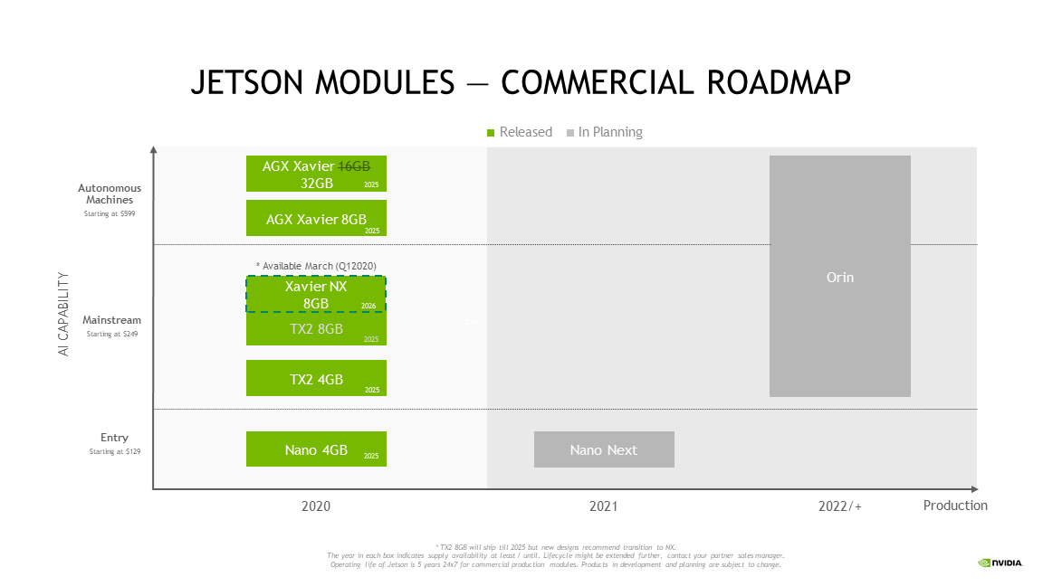
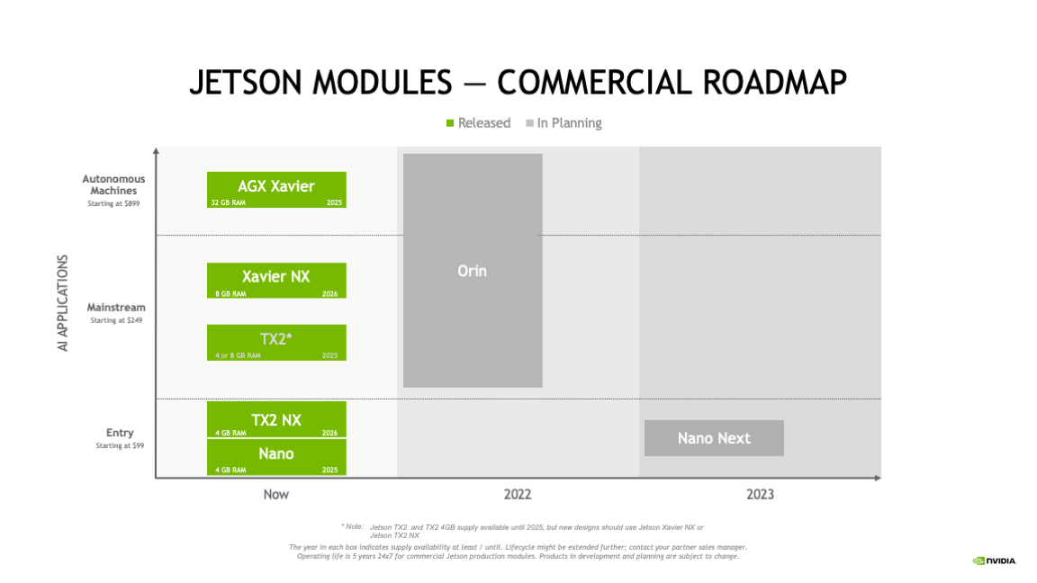
this image is probably the most proof we have of Dane being intended for 2021

Jetson_modules-Commercial_roadmap.png


Jetson_modules-Commercial_roadmap-202102.png
 
this image is probably the most proof we have of Dane being intended for 2021

Jetson_modules-Commercial_roadmap.png


Jetson_modules-Commercial_roadmap-202102.png
Yeah, seems Nano Next was either a victim of the chip shortages, Nintendo wanting to make it more within their specifications, or both.
 
0

Yep I remember the whole premium material thing of a magnesium alloy body was seen as a pipe dream when that DigiTimes article first came out and now the OLED definitely proves this is Nintendo's trajectory.
 
0
Although I will say, the Nano Next is 2023, and considering Dane likely will have a bit of exclusivity on its timing, that would indicate a 2022 release IMHO.
 
It specifically mentions just cpu.

Could Nintendo have considered pairing the tx1 gpu with a better cpu?
Could have been semantics and meaning a better SoC performance overall?
Maybe they were considering this(originally) for the OLED model though, it is Nintendo so better ARM CPU cores while having the GPU clocked higher as well could have been a decent upgrade.

It probably would have put the cost to close to where they might want to price the next Switch though to justify the upgrades...
It could have something to do with that rumour that Nvidia wanted to halt production of the Tegra X1 lineup this year, so a new SoC was going to be used in its place (likely on a smaller process to increase yield and happened to feature a better CPU), but TX1+ still being in the OLED suggests Nintendo and Nvidia worked something out on that front.
 
I just meant since the bc issue is specifically gpu related, could they have considered something like an a78 tx1 for the oled?
My guess is probably not, considering that 10 nm** is the oldest process node that the Cortex-A78 is optimised for.

But Nvidia could theoretically use the Cortex-A72, considering that Nvidia acquired Mellanox in 27 April 2019, and Mellanox did have a licence for the Cortex-A72.

** → a marketing nomenclature for all foundry companies
 
0
It could have something to do with that rumour that Nvidia wanted to halt production of the Tegra X1 lineup this year, so a new SoC was going to be used in its place (likely on a smaller process to increase yield and happened to feature a better CPU), but TX1+ still being in the OLED suggests Nintendo and Nvidia worked something out on that front.
It's very possible that this was just some confusion between the two different iterations of the chip, because the original TX1 that was in the hybrid Switch up until late 2019 was actually discontinued this year.

In general, though, I'm not sure I'd read too much into using the word CPU rather than the more correct SoC. A change in CPU implies a change in GPU since they're on the same die, and some of the people writing these articles probably aren't the most technical ever.
 
0
Does anybody know if the kemi on the new dock is 2.0, 2.0a or 2.0b?
to be honest i could see nintendo just not going for 2.1
2.0b supports 4k@60, hiher is unrealistic, and is also supports HDR (well, ned dynamic but it would be such a nintendo move)

the limiting factor of the interface is well known, usb-c (usb 3) has a limited bandwidth, there is a reason why they changed up the ubs slot for the eternet port. If you added a usb-> network adapter you have the same (still confused that i have read of people that wanted to buy the oled just for the new port…)

depending on the timing i could see them either embracing usb 4.0 if by then it gets more mainstream, or just sticking with the current setup… and i really hope that by then they have a 256gb option. 128gb in late 2022 on a 4k capable console that will cost at a minimum 350 would just be a joke…
 
Yeah, regardless of the expense to make it, I expect no greater than $350 unless inflation goes wild. If Nintendo takes no profit margin from hardware sales in its first year or so, so be it.
 
What's the price you guys are expecting Switch Dane?

I don't belive nintendo will output a $400+ System.

I think they were initially targeting for a 350€/$ figure, but they are ready for a slight bump up to 400€/$ depending on how inflation evolves, material availability, providers, contracts...
 
0
Does anybody know if the kemi on the new dock is 2.0, 2.0a or 2.0b?
to be honest i could see nintendo just not going for 2.1
2.0b supports 4k@60, hiher is unrealistic, and is also supports HDR (well, ned dynamic but it would be such a nintendo move)
Based on the specs of a similar chip (RTD2172U), the RTD2172N is very likely to be a DisplayPort 1.4 to HDMI 2.0b converter chip.
 
Based on the specs of a similar chip (RTD2172U), the RTD2172N is very likely to be a DisplayPort 1.4 to HDMI 2.0b converter chip.
Then i honestly would not expect the successor to have a different dock then the oled.
they‚re aiming for 4k upscaled with dlss, 120 just seems really unrealistic.
Except if a developer has a 1080@12p option as a performance mode.
 
I expect it to be in the $400usd area, and I expect to decide I don't really need it (I don't even have a 4k tv), but then I expect they'll announce it launching with a Zelda-themed limited edition design, and I expect I'll cave in record time. 😅
 
What's the price you guys are expecting Switch Dane?

I don't belive nintendo will output a $400+ System.
I think that even Nintendo doesn't know yet and is looking at the sales data of Switch against Switch OLED to decide. That's how I will know if I can relax my current belief of it not being above $300, and go to $350.
For now, that's $300 max and hardware tailored to fit in that price.
 
8 nm in 2022/2023 is less than ideal, so we already have that one covered.

I would agree if eletronics were getting cheaper over time, but times have changed.

I think that even Nintendo doesn't know yet and is looking at the sales data of Switch against Switch OLED to decide. That's how I will know if I can relax my current belief of it not being above $300, and go to $350.
For now, that's $300 max and hardware tailored to fit in that price.

I do hope they have an Standard Switch Dane if they are going to have an premium one (350+).
 
0
DLSS is all about supporting variable resolutions but still ensuring fidelity on higher resolution screens. Nintendo care about their games looking as intended on a screen and this is where the Wii began to struggle as people upgraded to HD.

Maybe they bump the Switches own resolution to 1080p but if I were Nintendo I would be tempted to just use the OLED screens already in my supply chain (I am not Nintendo just an FYI). The 4K benefit will be for docked and the original resolution will differ game to game, am sure some titles can achieve native but Nintendo will be using the extra power to push their games even further and utilise DLSS to make the, look great on any resolution screen.

I know they have their own tools but am still surprised no one went with Nvidia on the Sony/MS front.

Backward compatibility, well we’ll see I guess but we’ve seen hardware constraints are not as big an obstacle these days. I do get a bit confused why some people discussing this also like to discuss the next Switch as if it’s a pro version and not a next gen console - you can’t hand it be a Pro but not natively run Switch games.

Switch 2 will absolutely lead to improved performance, improved functionality and improvements in resolution/visuals. It’s not going to be running Doom on level with the Switch but at 4K. It is absolutely a next gen system so I think we’ll see similar patches to MS/Sony but maybe Nvidia will be able to drive some of this on their side. This might actually be a positive as Nintendo will be patching to run on the new hardware so would benefit from performance and resolution improvements.
 
Please read this staff post before posting.

Furthermore, according to this follow-up post, all off-topic chat will be moderated.
Last edited:


Back
Top Bottom