• Hey everyone, staff have documented a list of banned content and subject matter that we feel are not consistent with site values, and don't make sense to host discussion of on Famiboards. This list (and the relevant reasoning per item) is viewable here.
  • Do you have audio editing experience and want to help out with the Famiboards Discussion Club Podcast? If so, we're looking for help and would love to have you on the team! Just let us know in the Podcast Thread if you are interested!

StarTopic Future Nintendo Hardware & Technology Speculation & Discussion |ST| (Read the staff posts before commenting!)

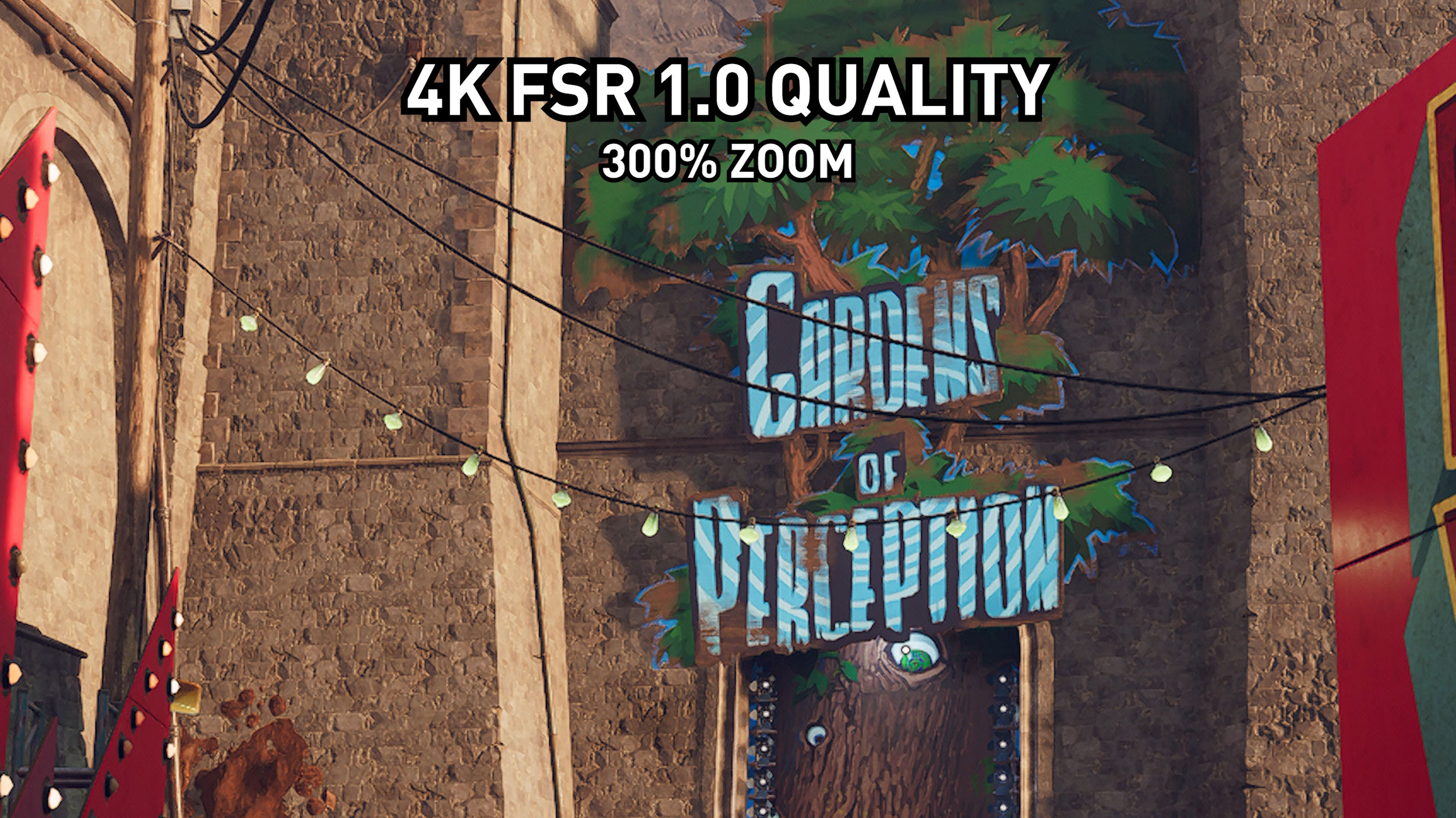
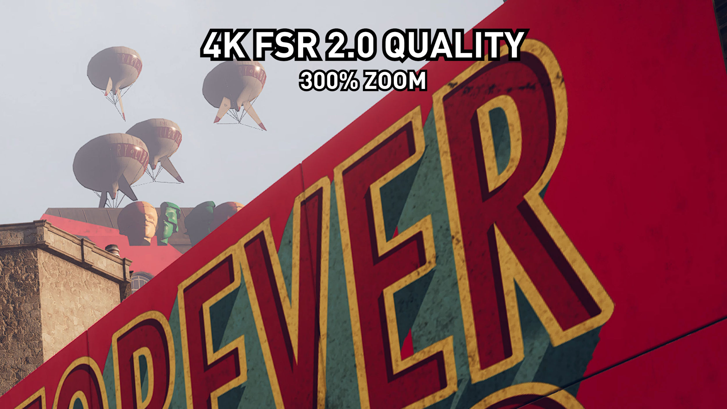
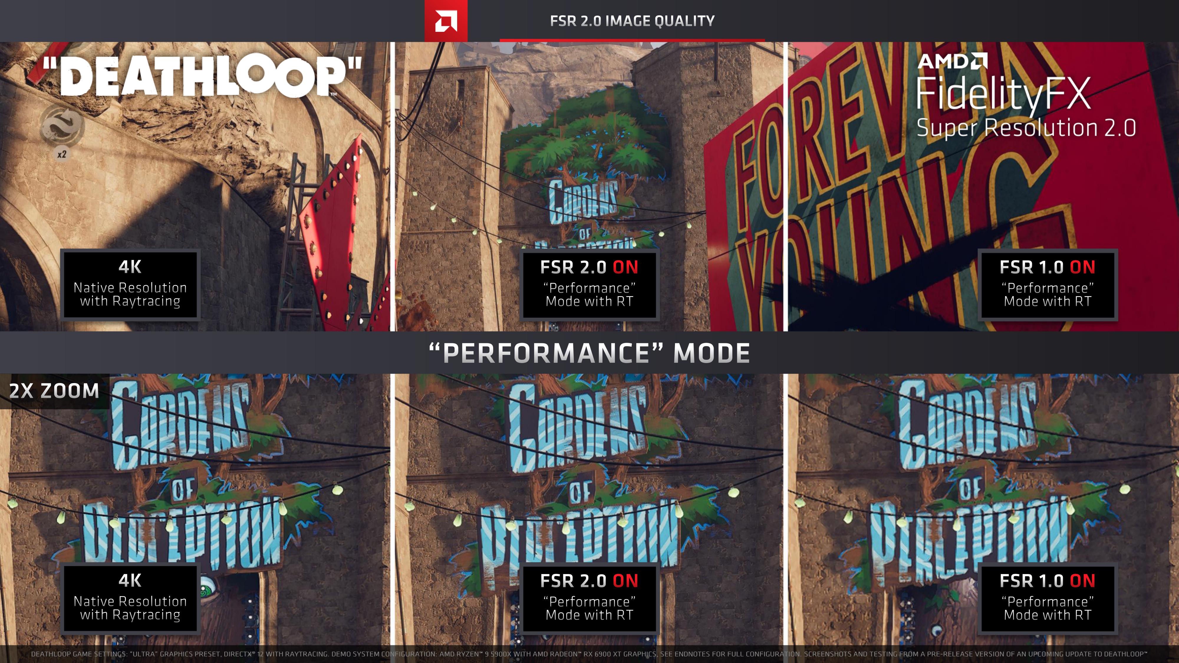
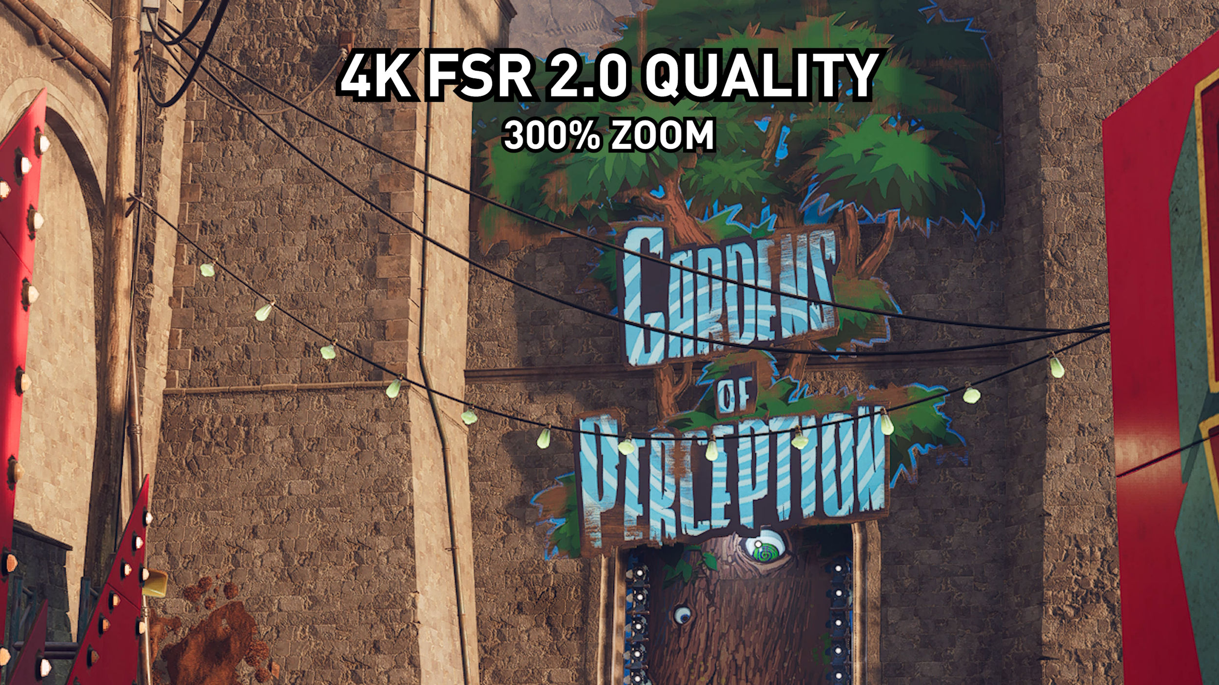
FSR 2.0 looking promising 👀

Dealthloop-1-NATIVE-.jpg
Dealthloop-1-FSR2.jpg
Dealthloop-1-FSR1.jpg


Deathloop-NATIVE.jpg
Deathloop-FSR2.jpg
Deathloop-FSR1.jpg


AMD-FSR-2.0-3.jpg
AMD-FSR-2.0-4.jpg


What's most impressive is the fact that it looks comparable to DLSS 2.0, yet doesn't need ML to train a model AND it stays open source. I wonder how it'll stack up against DLSS 2.0 when it releases and people start comparing the two. Also, would the performance hit be greater than DLSS?
I assume implementing FSR 2.0 will be similar to DLSS 2.0 because of the need for depth, motion vector, and color data?

Source pictures: https://videocardz.com/newz/amd-teases-fidelityfx-super-resolution-2-0-coming-q2-2022
Is it just me or does FSR2.0 actually look better than native? :oops:
 
There is absolutely no way…zero, none…that Nintendo would release an upgrade model at the halfway point of the Switch’s lifecycle, during its continued and upward growth, and position it as a next gen successor.

No way.
OK, but what this tells me is that they're not going to release such a model in 2020.
 
0
I am saying for the future
Like, after the launch for future models.

EX: Drake Lite

Drake is a next-generation model, and it will have to get treated as one in full once Mariko can no longer be produced.

So Drake's base cost can't be too high otherwise the Drake Lite will be too expensive/the gap between the Drake Lite and Drake-Hybrid will be too big.

Oh I see what you are saying.

Yea, I’m predicting low cost Mariko models will still be available to purchase until the next model after this new one is released.

When Nintendo says they plan on supporting/producing the current Switch system well beyond the normal ~10 year cycle…I believe them.

GTX 970 was crippled with having 0.5GB out of it’s 4GB ram to be really slow thanks to some shenanigans from Nvidia’s side.
Think it was the SM setup being very different from the 980 resulting in a big memory penalty when using more than 3.5GB of ram

What’s your definition of “crippled”?

The GTX 970 was insanely popular. And had crazy price/performance positives.
 
I don't know how this discussion suddenly became all about people's feelings over price, when I would expect them to know better than get emotional over estimates that are just pure speculation at this point...

Besides, I would advise against trying to spend on something outside one's financial means. This is the reason why I've held off on building a new PC, or buying every game that comes out. I simply lack the time and resources to enjoy everything nowadays.

The issue is the dismissive tone and elitist attitude regarding people's financial situations. These discussions don't happen in a vacuum; we're human beings and have emotions by nature.

It's ok to recognize the misfortunes of others from an empathetic perspective without arguing that Nintendo should base their business decisions on those misfortunes.

All I'm saying is that it sucks for poor gaming enthusiasts to not be able to by a new console that they might be excited about. It's just a basic expression of empathy that I didn't think would need this much explanation, quite frankly.
 
"Swivel block"?

Is this going to be like the FlipGrip, but in docked mode?
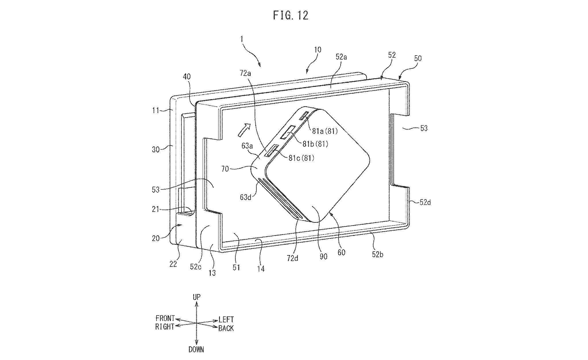
The swivel block is the portion at the back of the dock that has the power, HDMI and USB ports. The point of this is to allow it to swivel so that the wires can extend in whatever direction the end user needs for their particular setup.

It seems nice but it'll probably add too much to the cost for fairly little benefit. They seemingly also add an additional vent to this block part, but nothing else is really different.
 
0
So Nintendo filed an interesting patent regarding the dock on 12 July 2021, which was published on 20 January 2022.

I wonder if the DLSS model*'s dock could inherit some of the interesting features mentioned in the patent. (Although very unlikely to happen, I would personally like to see Nintendo release a smaller, more compact dock in the similar vein to the Insignia Dock Kit.)
"Swivel block"?

Is this going to be like the FlipGrip, but in docked mode?
For some reason I'm picturing something like this,

71LnwtVj9SL._AC_SX679_.jpg


But with the added bonus of being able to connect to a TV and all that other jazz. Stripping just about every use of plastic to only what's necessary. Which, I guess given recent oil prices, stands to make sense if they can cut costs in any way possible even if the more expensive components are silicon/electrical.


e: lmao
 
Last edited:
For some reason I'm picturing something like this,

71LnwtVj9SL._AC_SX679_.jpg


But with the added bonus of being able to connect to a TV and all that other jazz. Stripping just about every use of plastic to only what's necessary. Which, I guess given recent oil prices, stands to make sense if they can cut costs in any way possible even if the more expensive components are silicon/electrical.
We have images of this in the patent document, it's just a normal dock with this swivel block of connectors on the back:

FJkWFVTWYAAtuLd
 
We have images of this in the patent document, it's just a normal dock with this swivel block of connectors on the back:

FJkWFVTWYAAtuLd
Oh shit, I feel dumb 😅 When I clicked the images link I was just taken to a PDF that showed the front of the Switch dock and it looked identical to the existing dock. Don't mind me then lol
 
I'm actually a bit unclear on why cache size correlates to slowdown. Is it because of the time necessary to search through the increased cache? Is it because the increase in physical size increases the average distance from CPU to the cache (and we're still bound by the speed of light)? Is it a combination of both?
I’m unclear myself I only know it from the Nvidia paper. But the latency drop measured is 1%
 
0
Oh shit, I feel dumb 😅 When I clicked the images link I was just taken to a PDF that showed the front of the Switch dock and it looked identical to the existing dock. Don't mind me then lol
Yeah that website feels kinda antiquated, it's kinda hard to navigate the images. I prefer to use Google patents personally.
 
The issue is the dismissive tone and elitist attitude regarding people's financial situations. These discussions don't happen in a vacuum; we're human beings and have emotions by nature.

It's ok to recognize the misfortunes of others from an empathetic perspective without arguing that Nintendo should base their business decisions on those misfortunes.

All I'm saying is that it sucks for poor gaming enthusiasts to not be able to by a new console that they might be excited about. It's just a basic expression of empathy that I didn't think would need this much explanation, quite frankly.
You do have to consider that there are many factors outside of many people's control right now, such as the ongoing conflict in Ukraine, the global chip shortage, economic inflation, and other things that will ultimately determine price points.

One could make the same argument that Apple is "apathetic" because their latest models of the iPhone SE is considerably more expensive than the previous iteration (the SE 2nd Gen/2020), when sourcing parts have gotten considerably more expensive due to the aforementioned reasons. I don't think companies will suddenly be running a charity just because the newer price points are less considerate the lower end/lower income bracket (though they do have payment installment plans if that helps...perhaps Nintendo should consider looking into that for certain regions but that would be a whole other issue to sort out...).

At the end of the day, companies are companies, and they will always be in the business of making a profit, regardless of people's feelings. I don't think pricing it high will be any less considerate considering how games and other consoles are currently priced right now. Yes, it's a shame.

And just to be clear: I'm not being dismissive about people's financial situations. Video game consoles are considered a luxury, and if one's current financial situation make it prohibitive, there are still free alternatives such as mobile and free-to-play games. That said, it's recommend that one should secure the means to have a sustainable livelihood, and video games may not necessarily constitute such needs.
We have images of this in the patent document, it's just a normal dock with this swivel block of connectors on the back:

FJkWFVTWYAAtuLd
What are those slots on the bottom?

New media perhaps? Ventilation?
 
Last edited:
So Nintendo filed an interesting patent regarding the dock on 12 July 2021, which was published on 20 January 2022.

I wonder if the DLSS model*'s dock could inherit some of the interesting features mentioned in the patent. (Although very unlikely to happen, I would personally like to see Nintendo release a smaller, more compact dock in the similar vein to the Insignia Dock Kit.)

Didn't read into it much, but it sounds like it's trying to address HDMI/cables coming out of one side when your TV is on the opposite - calling it 'troublesome'
 
0
They're additional air vents. As far as I can tell that's the only other additional thing.
Will these newer docked perhaps have a pass-through fan? Perhaps the dock has a built-in one to aid as well?

If that's the case then we are going to be seeing some very interesting docked clocks...
Is it just me or does FSR2.0 actually look better than native? :oops:
Same. I think Nintendo might have found their solution for extending the (base) Switch's life span a little further.

Which in turn gives credence to this new "successor" model being teired as a premium device.
 
Will these newer docked perhaps have a pass-through fan? Perhaps the dock has a built-in one to aid as well?

If that's the case then we are going to be seeing some very interesting docked clocks...

Same. I think Nintendo might have found their solution for extending the (base) Switch's life span a little further.

Which in turn gives credence to this new "successor" model being teired as a premium device.
To be clear, it's very unlikely that the dock described in the patent application is ever something that they will be selling. It likely wouldn't have been published if they planned to announce it later.

And according to this description there is no fan or any sort of active cooling going on in the dock. It's just an additional set of vents on this block probably because the block is now going to be sealed off in order to allow the whole thing to be swiveled.
 
Quoted by: SiG
1
To be clear, it's very unlikely that the dock described in the patent application is ever something that they will be selling. It likely wouldn't have been published if they planned to announce it later.

And according to this description there is no fan or any sort of active cooling going on in the dock. It's just an additional set of vents on this block probably because the block is now going to be sealed off in order to allow the whole thing to be swiveled.
I can't help but think this dock would come with VESA mounts, especially if it's meant to swivel around.
 
0
You do have to consider that there are many factors outside of many people's control right now, such as the ongoing conflict in Ukraine, the global chip shortage, economic inflation, and other things that will ultimately determine price points.

One could make the same argument that Apple is "apathetic" because their latest models of the iPhone SE is considerably more expensive than the previous iteration (the SE 2nd Gen/2020), when sourcing parts have gotten considerably more expensive due to the aforementioned reasons. I don't think companies will suddenly be running a charity just because the newer price points are less considerate the lower end/lower income bracket (though they do have payment installment plans if that helps...perhaps Nintendo should consider looking into that for certain regions but that would be a whole other issue to sort out...).

At the end of the day, companies are companies, and they will always be in the business of making a profit, regardless of people's feelings. I don't think pricing it high will be any less considerate considering how games and other consoles are currently priced right now. Yes, it's a shame.

And just to be clear: I'm not being dismissive about people's financial situations. Video game consoles are considered a luxury, and if one's current financial situation make it prohibitive, there are still free alternatives such as mobile and free-to-play games. That said, it's recommend that one should secure the means to have a sustainable livelihood, and video games may not necessarily constitute such needs.

I'm not making any arguments about companies being apathetic. They're business entities. I don't expect them to care about people. I'm talking about people in this thread acting like it's bad for poor people to want nice things or for others to feel bad that they can't have nice things. That's literally my only point here.
 
The "double speed" thing is marketing relative to Volta. Chips starting with Turing doubled the FP16 performance compared to Volta. Ampere then doubled the FP32 performance, making them 1:1 again. Orin is unique among the Ampere chips because it again doubles the FP16 performance, making it 2:1 with FP32. Drake doesn't seem to have this feature.
If I’m not mistaken, but Volta and Turing process the FP16 at double the rate of FP32, so a 2:1, and I’m not sure if it really counts as marketing per se since it went from 64cores per SM in Turing to 128 cores in Ampere from doubling the 32. I think there’s also the option to do 1FP32 and 2FP16 if a developer chooses to in Ampere, but I may have just interpreted that part of the information incorrectly.

I see. So the cache minimizes the 'backtracking' of data between the CPU and GPU and the RAM/storage. So, the more often a certain data is used, the closer it must be placed to make the cache as efficient as possible.

OK then, cache is there to boost performance. And a difference in cache can explain why Nvidia flops are not equal to AMD flops? If yes, how did that change with the introduction of Infinity cache. And is this cache an L3? So it is inherently slower than any L1 and L2 cache around, yes?

Sorry for asking so many questions but this board has a very pedagogic approach to explaining this stuff and I can't stop learning. It's a great feeling.
I think best not to focus on the FLOPs as it is a way to confuse you more. With FLOPs they are theoretical floating point operations it can do per second. The 3090 can do 35TFLOPs FP32 while 6900XT can do only 23TFLOPs FP32. The 3090 can also do 35TFLOPs FP16, and the 6900XT can do 43TFLOPs FP16. Pretty nice numbers… that mean nothing. These two cards are within a stone’s throw of each other, like 10% in performance (non-RT).

This is where it gets even muddier, it’s mostly useless to compare the TFLOPs of two different architectures, as the 3090 TFLOPs only, and I should stress only, makes sense when you compare it to the other cards in the Ampere lineup of GPUs. RDNA2 TFLOPs only make sense when comparing it to the other RDNA2 TFLOPs.

The reason NV flops and AMD flops is dependent on a game by game basis. RDNA2 is an engine so to speak, it’s is a powerful raster engine and a game like Halo Infinite will perform better on the RDNA2 engine than on the Ampere engine.

Ampere is another engine, a powerful Ray Tracing and Machine Learning engine that has superb performance in a title such as Metro Exodus or Cyberpunk 2077 when RT is enabled. And it doesn’t need DLSS all the time to be better than the RDNA2 counterparts in RT🤭

This time around, AMD is the one that is noted as having the more efficient TFLOPs, simply due to the fact that they’ve managed to keep their powerful raster engine fed with data more often than not with their cache setup, having to not fetch from the VRAM so often (which requires wasting energy especially for the smaller tasks) is what aided their efficiency along with the engineering to have a higher clock speed.

NV didn’t do that, but judging by leaked information they seemed to be doing just that for Lovelace which is to have a larger amount of Cache (no L3 though), however they are also relying on the very power hungry GDDR6X and clocking their GPUs crazy high that mitigate their efficiency gains.


The way I think of cache is like a library, you have one of the librarians and she is stamping books that are verified to be read again and those that are returning. She checks the database and sees that one of the books, in this example War and Peace, was supposed to return to the library 2 weeks ago. So, she sends out one of the assistants to check in level 1 because the librarian already checked level 0 which is deep in the basement. The assistant goes to level 1 that’s much larger than level 0 and has stacks of books, can’t find it so now they have to go to level 2 which has even more books and some readers in there, level 2 has hundred upon hundreds of books. Nothing. Then there’s level 3, which is the floor everyone can access and this has thousands of books that have to searched through, even the pile of books that are returned. There isn’t anything.


Turns out War and Peace is still at the home of the user who signed it out and it’s ruined, they pay that fee for ruining the book but a new book has to be ordered from the Bookstore VRAM to replace this. Make the call, do the order, and wait a few days to find this copy of the book.

Now they have to take this book down to the librarian so that she can stamp it and give it the greenlight for “Ready to use” in which the next reader can sign it out.


If that makes any sense. Not quite literally, but the general idea of levels.[/spoiler]
 
If I’m not mistaken, but Volta and Turing process the FP16 at double the rate of FP32, so a 2:1, and I’m not sure if it really counts as marketing per se since it went from 64cores per SM in Turing to 128 cores in Ampere from doubling the 32. I think there’s also the option to do 1FP32 and 2FP16 if a developer chooses to in Ampere, but I may have just interpreted that part of the information incorrectly.
The reason I say it's marketing is the practice to keep calling it "double rate FP16" even in Ampere when the doubling happened multiple microarchitectures ago, and (outside of Orin) didn't happen again with Ampere. And now that I look back at a chart that was posted in Discord, they were actually comparing it to Pascal. So it's a bit like "high-speed Internet" at this point.
 
Not that I’ll be buying it, but there’s this AAA game from Warner Bros, that is launching this Holidays and is apparently coming to Nintendo Switch in native form, as it has a physical edition.


The game might be using Unreal Engine, but I think it must be pretty scaled back to run in current Switch models.
 
Last edited:
Probably depends on how early/late into the design process.
Bus width would have to be pretty early, as that's related to the physical design. Like the actual number of physical pins used, IIRC.
Bandwidth.... well, bandwidth is memory frequency x 2 (because the DDR in DDR/LPDDR/GDDR stands for Double Data Rate) x bus width (usually in bits) / 8 (to convert to bytes). That's in MB/s, then divide by another ~1000 to get GB/s. So current Switch when docked is 1600 MHz * 2 = 3200 MT/s (MT = MegaTransfers), then x 64 / 8 = 25,600 MB/s, then divide by 1000 to get 25.6 GB/s. So, bus width as noted above is related to physical design, so that needs to be decided earlier. (Officially supported) maximum frequency/clock rate is decided by the particular memory standard/generation (LPDDR4 vs 4X vs 5 vs 5X, etc.). Which standard/generation is supported is in turn decided by the memory controller; presumably that too is figured out earlier in the process. The actual frequency/clocks at runtime should be decided on the software side, so that can come later.
Capacity... is indirectly constrained by bus width. Memory manufacturers produce RAM in chips or modules that are X bits wide with Y capacity. So when you decided on bus width, you effectively decided the minimum and maximum capacity as well, depending on what options RAM makers offer. But that's the range; your actual selection from the given options can come later, like with the Capcom example. Changing from 2 or 3 GB to 4 GB is a matter of changing from a pair of 32-bit 1 or 1.5 GB modules to a pair of 32-bit 2 GB modules. I say pair in this case as we've seen from teardowns that the Switch uses two modules, right? Anyway, that should be a relatively simple change that shouldn't require modifying the design.
So in order to increase a fixed quantity of RAM during the design phase (and more RAM is always better as one poster mentioned), the only prerequisite is to have settled for a certain die size, respectively a memory bus width. And that makes the bus width a very critical quantity. So, in the case of the succ, since we know that the hardware is pretty much constrained to some form factor, then the first thing we would check on would be that I assume, since it helps us calculate output of the GPU. Then we would be interested in the memory clock, and then in the possible VRAM configurations (if not straight up mentioned). Finally, we would turn our eyes to the CPUs but those are bound to not be a surprise given ARM-dominance in the low power space.

All of that in that order, correct? Assuming the CPUs will not bottleneck the GPU (which is a whole other topic).
The funny thing is TFLOPs are not comparable across generations even within the same vendor unless the core structure is VERY similar (Kepler 600 vs Kepler 700, Maxwell vs Pascal.etc, all the GCN-Gen cards more or less)


It's moreso of a quirk on how they calculate the TFLOP value and how that applies in real-world scenarios.


As for RDNA2, Infinity cache managed to bring the gaming FLOP efficiency up to a degree where it overtakes Ampere's FLOP efficiency.

RDNA2 without Infinity cache is either slightly less efficient, or marginally more efficient than Ampere per-FLOP.

As for Cache speed, yeah, L1 > L2 > L3 in speed, but cost increases greatly along with the size decreasing greatly as well usually.
So FLOPS are the last thing we should get interested in since we have no Lovelace GPU on the market with which we can compare the existing line-up of cards of Maxwell. Unless, that is, there is a way to easily factor in the cache configuration in our calculations, and so produce meaningful hypotheses.
You're asking a bunch of foundational questions about computing, which is rad. This is starting to get way off topic, but I'm gonna try and generalize a bit for you.

The basic loop that any computational system has is Take Some Data In -> Transform It -> Output. This structure is everywhere. You see it at the high level - how do I take the game data off the cartridge, turn it into a big open world, and shove it out to the screen - but it repeats at the low level of every individual component. I have to feed data from the cartridge and decompress it into memory, I have to get data into memory and put it in the processor, or the the GPU. Every output turns into an input for the next stage, into it finally turns into something that the player experiences... and then even the player experience turns into a button press, which becomes input again.

Every time we reproduce this pipeline, we ask the same kind of performance questions about it.
  • How do we make the loop faster, faster being measured by the number of times we can read/transform/output data in a second
    • When you see things like a clock speed or FLOPS (floating point operations per second), that's what we're measuring
  • How do we make this loop more performant, which is harder to have an objective measure of, but basically its how many times do we have to run this loop before we get the final result
    • When we talk about one microarchitecture being more performant per FLOP that is what we mean. If we can do more work per cycle, then we don't always need as many cycles-per-second
  • How do we make the cycles fatter or have higher bandwidth - how much data can we move in and out per second.
    • This is the bus speed we've been discussing
  • How do we make this loop shallower or less latent. So you might have a process that runs very fast and is ultra performant but has a long startup time.
    • Happens all the time in controllers. You want the response to be instant
  • How do we keep this loop fed or free from bubbles.
    • If one part of the system is waiting on another part, it doesn't matter how fast/efficient/latent/fat your pipe is
    • Making this work is often the job of the software devs
    • But they only have the tools available that the hardware gives them
    • Which is why some games can seem smaller than Doom/Witcher III to port to Switch, but devs can't make it work.
You can almost always make some part of the system BIGGER - more clock, more ram, more bus - but all of them cost money. And generate heat. And use battery. And take up space. So a hardware designer's job is often to figure out the biggest bang for the buck - which means looking at where software is hitting roadblocks now but also guessing what future roadblocks might be.

They've got a lot of tools to try, too. They can do things like:
  • JUST MAKE IT BIGGER. Valid, when you can do it, but you're quickly going to hit diminishing returns unless you make everythingbigger - the bus, the RAM, the GPU. That's why you can't just compare clocks between two systems and know which is "better"
    • Also, eventually you're going to be limited by the speed of light
  • Just add another one.2 cores instead 1, 4 cores instead of 2. This means you can do two things at the same time, but it only works if the kind of things you are doing can be split into independent tasks.
    • Like doing sound on one core, and physics on another.
    • Going to max out when you can't subdivide tasks anymore
    • Same goes for busses - two slightly slower busses might be better than one really fast bus, but only as long as you can split your data into two channels
  • Make it more complicated by specializing. For example: we used to do graphics on the CPU before the invention of the GPU! Then we invented this specialized piece of hardware to make just graphics faster.
    • But now we've added a second, inner cycle, where instead of just feeding the CPU, which goes to the screen, the CPU feeds the GPU, and sometimes it even comes backto the CPU. New spot for bubbles to occur...
      • And then a new spot to optimize this cycle again...
    • Only accelerates one part of the pathway. So if you CPU is crap, you maybe pushing gorgeous 3D worlds, but your physics and enemy AI is stuck in N64 era.
  • Make it more complicated by caching. Caching essentially lets you eliminate or greatly speed up one of the steps of the process. You have a tiny, expensive , blisteringly fastpiece of storage and you stick it inside one of the steps
    • For data input, you store the last couple things you looked at, so if you're still working on the same data, you don't actually have to read it again
    • For transformation you store the results of some instructions, and instead of doing the work again, when you see an identical instruction you just send out the old result
    • For output, you just cache the last thing you saw and use it again
      • Practically speaking what really happens isn't that you cache your output, it's that your output is someone else's input, so they do the caching
Okay, at this point I've written the intro to a hardware 101 textbook.
Give this champion its prize!

@Dakhil, could you threadmark this post? I guess a lot of us that are laymen in this domain but still have an interest in it will greatly appreciate this contribution.

It's an excellent post @oldpuck. Thank you for the love.
Cache gets slightly slower the bigger it gets. If your system has a working set small enough that it fits in the smaller cache, the newer, bigger cache can cause problems.

In the Big Data server workloads I am used to that is almost never a problem. I suspect that video games have similar bigger-cache-is-better-cache workloads, but are also very sensitive to latency problems
I guess this must be true since the CPU has more boxes to check to find the data it's looking for but then I assume this is also true for any memory type? The bigger the RAM quantity the slower it will be because the CPU has more indexes to look through? So, 16 GB of RAM will always be slower than its 8 GB counterpart?
Functionally speaking, yea, Infinity Cache is just a fancy name for L3. It's a level of cache placed after L2, ergo it's L3 (because the naming is descriptive).
It would be slower relative to L1 or L2, because I think that it'd be physically located further away than the L1 or L2 are.


I'm actually a bit unclear on why cache size correlates to slowdown. Is it because of the time necessary to search through the increased cache? Is it because the increase in physical size increases the average distance from CPU to the cache (and we're still bound by the speed of light)? Is it a combination of both?

And to answer 'downsides of such enormous caches': die size. Cache/SRAM is the opposite of dense.
Although honestly, I'm a bit unclear myself on how the gap in density between SRAM and DRAM is so big. I get that a SRAM cell needs 6 transistors while a DRAM cell needs 1 transistor + 1 capacitor. I'm... not sure how we eventually get to 'cache is measured in KB/MB, RAM modules are in GB'.
I do get on the surface level that in manufacturing, logic has been shrinking faster than SRAM, but I'm unclear on specifics.
I have a feeling that cache might be the succ's 'secret sauce' along with RTX and machine learning cores. The more we learn about it the better. That said, although I kinda understand why a cache should not be big and why the physically closest cache must preferably be the fastest too, I still fail to see why you would increase a cache size that is lower ranked? Unless you have to because it is shared with other components that necessarily further away from the CPU? But then, what is the point in a SoC like the succ's in which CPU and GPU have access to the same memory pool?

I think I am close to reaching a satisfactory level of knowledge about the design of SoCs. I thank everyone for being so great at explaining stuff.
 
Last edited:
If I’m not mistaken, but Volta and Turing process the FP16 at double the rate of FP32, so a 2:1, and I’m not sure if it really counts as marketing per se since it went from 64cores per SM in Turing to 128 cores in Ampere from doubling the 32. I think there’s also the option to do 1FP32 and 2FP16 if a developer chooses to in Ampere, but I may have just interpreted that part of the information incorrectly.


I think best not to focus on the FLOPs as it is a way to confuse you more. With FLOPs they are theoretical floating point operations it can do per second. The 3090 can do 35TFLOPs FP32 while 6900XT can do only 23TFLOPs FP32. The 3090 can also do 35TFLOPs FP16, and the 6900XT can do 43TFLOPs FP16. Pretty nice numbers… that mean nothing. These two cards are within a stone’s throw of each other, like 10% in performance (non-RT).

This is where it gets even muddier, it’s mostly useless to compare the TFLOPs of two different architectures, as the 3090 TFLOPs only, and I should stress only, makes sense when you compare it to the other cards in the Ampere lineup of GPUs. RDNA2 TFLOPs only make sense when comparing it to the other RDNA2 TFLOPs.

The reason NV flops and AMD flops is dependent on a game by game basis. RDNA2 is an engine so to speak, it’s is a powerful raster engine and a game like Halo Infinite will perform better on the RDNA2 engine than on the Ampere engine.

Ampere is another engine, a powerful Ray Tracing and Machine Learning engine that has superb performance in a title such as Metro Exodus or Cyberpunk 2077 when RT is enabled. And it doesn’t need DLSS all the time to be better than the RDNA2 counterparts in RT🤭

This time around, AMD is the one that is noted as having the more efficient TFLOPs, simply due to the fact that they’ve managed to keep their powerful raster engine fed with data more often than not with their cache setup, having to not fetch from the VRAM so often (which requires wasting energy especially for the smaller tasks) is what aided their efficiency along with the engineering to have a higher clock speed.

NV didn’t do that, but judging by leaked information they seemed to be doing just that for Lovelace which is to have a larger amount of Cache (no L3 though), however they are also relying on the very power hungry GDDR6X and clocking their GPUs crazy high that mitigate their efficiency gains.
I have a small problem with the bolded parts. I thought every CUDA core across the generations were delivering the same output at equal frequencies? So the only difference between Fermi and say Lovelace GPUs was the process node and memory configuration? Basically, you would gain performance by shrinking the CUDA cores and add more of them on the die and do clever stuff with the memory pools to speed up data transfers and voilà, you have a new generation? Are we somewhat both right?

I also thank everyone who mentioned the 'bubbles' in their explanation because I think this is something that is vastly overlooked and can account for the major differences in power computing we see in the market across all vendors.
The way I think of cache is like a library, you have one of the librarians and she is stamping books that are verified to be read again and those that are returning. She checks the database and sees that one of the books, in this example War and Peace, was supposed to return to the library 2 weeks ago. So, she sends out one of the assistants to check in level 1 because the librarian already checked level 0 which is deep in the basement. The assistant goes to level 1 that’s much larger than level 0 and has stacks of books, can’t find it so now they have to go to level 2 which has even more books and some readers in there, level 2 has hundred upon hundreds of books. Nothing. Then there’s level 3, which is the floor everyone can access and this has thousands of books that have to searched through, even the pile of books that are returned. There isn’t anything.


Turns out War and Peace is still at the home of the user who signed it out and it’s ruined, they pay that fee for ruining the book but a new book has to be ordered from the Bookstore VRAM to replace this. Make the call, do the order, and wait a few days to find this copy of the book.

Now they have to take this book down to the librarian so that she can stamp it and give it the greenlight for “Ready to use” in which the next reader can sign it out.


If that makes any sense. Not quite literally, but the general idea of levels.[/spoiler]
Dude, this is general relativity stuff. But I get the general idea; all the hentai would be stored in Level 0 because that is what the most in demand, while the architecture and and biology books are left to rot in Level 3.
 
Not that I’ll be buying it, but there’s this AAA game from Warner Bros, that is launching this Holidays and is apparently coming to Nintendo Switch in native form, as it has a physical edition.


The game might be using Unreal Engine, but I think it must be pretty scaled back to run in current Switch models.


Could this be one of the games from the devs that have the new hardware kits?
 
It's more probably a Quick and dirty port, it makes totally sense to release this franchise on switch, no matter how crappy it runs...
One dosent exclude the other.

It’s definitely possible they had a 4k dev kit. It’s also possible they didn’t. That also applies to every game coming out in the latter half of 2022.
 
I have a feeling that cache might be the succ's 'secret sauce' along with RTX and machine learning cores. The more we learn about it the better. That said, although I kinda understand why a cache should not be big and why the physically closest cache must preferably be the fastest too, I still fail to see why you would increase a cache size that is lower ranked? Unless you have to because it is shared with other components that necessarily further away from the CPU? But then, what is the point in a SoC like the succ's in which CPU and GPU have access to the same memory pool?

I think I am close to reaching a satisfactory level of knowledge about the design of SoCs. I thank everyone for being so great at explaining stuff.
Because even the lowest ranked Cache is much, much faster than any RAM.

During my college years, I remember looking at the specs of the local supercomputer I left underwhelmed by the CPU specs... The CPU speed was lower than 200Mhz, at a time where personal devices with Pentium III were approaching 1Ghz. I wanted to know why even using only 1 core was much faster than my personal device. That's when I learned that the CPU had an enormous (for the time) 8MB L2 cache. My Pentium III was closer to 256KB. That's what you get with a multimillion device in the early 2000's.
 
Last edited:
0
Not that I’ll be buying it, but there’s this AAA game from Warner Bros, that is launching this Holidays and is apparently coming to Nintendo Switch in native form, as it has a physical edition.


The game might be using Unreal Engine, but I think it must be pretty scaled back to run in current Switch models.

let's see which studio is working in the hogwards legacy port

maybe Saber? Or Virtuous?
 
0
There is absolutely no way…zero, none…that Nintendo would release an upgrade model at the halfway point of the Switch’s lifecycle, during its continued and upward growth, and position it as a next gen successor.
No way.

Now, you can argue with me all you want that Nintendo will eventually treat Drake Switch as a successor and stop selling and supporting OLED/Lite/older hybrid Switch’s In two years…go ahead and do that. But they absolutely won’t release it as such.

So suggesting they will call it Switch 2…or that they need to…is just silly. No offense :p

Actually its silly to say "absolutely no way…zero, none…" because nothing is confirmed or certain about this new Switch hardware, and that including positioning (even Nate said that he is not sure how Nintendo will positioning it).
But it has much more sense that if Nintendo really is releasing basically next gen hardware (based on rumors), to positioning it more like next gen Switch instead of simple upgrade.

No one said that they need to call it Switch 2, but if its really next gen Switch hardware and Nintendo want to positioning like that,
Switch 2 naming has plenty of sense, because Switch 2 naming tells very simple and clear its next gen Switch console.

So actually you are being silly because you think what I wrote is silly. :D
 
Last edited:
Well, this is interesting: Hogwarts Legacy listed on Amazon for Switch.

Yes this could be a cloud version, but if it's not, would certainly be an awesome Switch 2/Pro/4K/YoMama game to show the device off, since it's a looker.
 
0
One dosent exclude the other.

It’s definitely possible they had a 4k dev kit. It’s also possible they didn’t. That also applies to every game coming out in the latter half of 2022.

Ho yes, of course.
My comment was more something like don't assume a new model is coming this year because of the release of this game...
 
0
Nintendo likes to operate in tick-tock model GB - GBC - GBA (15 years), NES - SNES (13 years), DS - 3DS (12-13 years), NGC - WII - WII U (15 years). If they speak about Switch being in the middle of its life cycle it could mean that there will be a "tock" and OG Switch will have a few years of life. It is impossible for the GA10F to be so powerful just to upscale to 4K. The SOC is so much better that the OG Switch is too much of a development bottleneck.
 
0
I could see Hogwarts having a Switch 4k upgrade if the console is indeed coming within the next year, maybe that’s why they have been quiet about a Switch version? It’s interesting though as it’s not something I expected to see running on Switch.
 
The reason I say it's marketing is the practice to keep calling it "double rate FP16" even in Ampere when the doubling happened multiple microarchitectures ago, and (outside of Orin) didn't happen again with Ampere. And now that I look back at a chart that was posted in Discord, they were actually comparing it to Pascal. So it's a bit like "high-speed Internet" at this point.
I’m not saying it necessarily is new to Ampere, just that it’s executed a bit differently than it was in the past, ie im implying it was done back then as well.

Really it’s the FP32 that is technically done differently, the FP16 is done the same.

I have a small problem with the bolded parts. I thought every CUDA core across the generations were delivering the same output at equal frequencies? So the only difference between Fermi and say Lovelace GPUs was the process node and memory configuration? Basically, you would gain performance by shrinking the CUDA cores and add more of them on the die and do clever stuff with the memory pools to speed up data transfers and voilà, you have a new generation? Are we somewhat both right?

I also thank everyone who mentioned the 'bubbles' in their explanation because I think this is something that is vastly overlooked and can account for the major differences in power computing we see in the market across all vendors.
CUDA is a programming language and the NVidia cards for a long time have cores that run CUDA. However, the microarchitecture that encompasses the cores is different.

Ampere for example has a 128 CUDA cores per SM, while Turing has 64 CUDA cores per SM.

There are other changes as well to the cache, ROPs, TMUs, and other features that were added or changed. Turing for example has 8 Tensor Cores per SM, but Ampere only has 4 tensor cores per SM and they are the 3rd generation of Tensor Cores while Turing has 2nd generation.

This is what makes up the architecture and what differentiates one from the other. They all run CUDA yes, but they are not all equal cards. The layout of how the card is differs from one generation to another, but the core ability to run CUDA is still there.


Dude, this is general relativity stuff. But I get the general idea; all the hentai would be stored in Level 0 because that is what the most in demand, while the architecture and and biology books are left to rot in Level 3.
This is an interesting way to put it 🤣
 
Wow Legacy is coming to Switch? The heck I never saw that coming. Now this feels like a top candidate game coming to this next Switch iteration. Warner Bros having a dev kit makes sense.
 
Last edited:
Nintendo could price it at 999 but the point is they will not because the hardware is means to sell their 60 dollar software. As they said multiple times, they are an entertainment company in a business where subsidizing hardware is the game. The switch made little profit but not Apple-like profit. A drop in the profit margin of OLED could be because it is a new product with a new manufacturing line, it costs some money per product.
The SOC won't be that expensive if it is manufactured on 8 NM (cheaper than anything TSMC or Samsung 5NM) and there is a notable difference between T234 and T239: T239 doesn't have double speed FP16 processing which means it will have a transistor budget of GPU portion of SOC akin to 1/7th of GA102 (4 to 5 billions transistors). It could be a 180 mm2 (max) SOC fitting a tablet form factor and if they decide that in handheld mode it will run only half of SMs, they could bin the SOC for a handheld only version.
iPhone 12 has under 400 dollars BOM with 90 dollars 5G modem and expensive display.

I've been doing a bit of research into this, and I'm actually not sure that the bolded is correct. Samsung 8N is surely the cheapest plausible node per wafer, but once you take into account density and yields, it's entirely possible that a more advanced node like TSMC N5 is actually cheaper per chip. In fact, my back-of-a-paper-envelope maths suggests that a Samsung 8N Drake could cost 70% more than a TSMC N5 Drake.

I should emphasise that I have no expertise in this field, my analysis contains a lot of assumptions and estimations which may deviate significantly from reality, and you shouldn't take what I'm about to write any more seriously than any other random person on the internet. That said, I can run through the maths of it.

A few pages back, I posted an estimate of Drake's die size on various manufacturing processes. I've revised my estimates on these figures in two ways since then. The first is that I'm now estimating Drake's transistor count to be around 8 billion transistors. This is based on Nvidia's Orin die photo actually being for an older 17 billion transistor configuration of the chip, but also from the fact that Xbox Series S's "Lockhart" SoC reportedly comes in at 8 billion transistors itself. This is the same number of CPU cores (8) and GPU shader "cores" (1536) on the silicon as Drake, but we know that the Zen2 CPU is larger and uses more transistors than A78, and RDNA2 similarly is larger and uses more transistors per "core" than Ampere. There are some differences between Drake and base Ampere, though, the 4MB of L2 cache will add considerably to the total (based on the GA102 die, it looks like it could be around 1.3 billion transistors for that alone), and there might be some additional components on there care of Nvidia that Nintendo don't really need, but might be useful for Nvidia's other customers (eg an 8K codec block). I'm just going with 8 billion as a round figure, but again there's a large margin of error.

The second change is that I'm changing my estimate for TSMC N7->N6 density improvement from 18% (TSMC's claim) to 8.1% (actual measured improvement from Navi 23 to Navi 24). That being the case, my new estimates are as follows:

ProcessDensity (mT/mm2)Drake size (mm2)
Samsung 8nm45.6175.4
Samsung 7nm59.2135.1
Samsung 5nm83.495.9
Samsung 4nm109.772.9
TSMC N765.6122.0
TSMC N670.9112.8
TSMC N5106.175.4

In terms of cost per wafer, my starting point was the figures shown in Ian Cutress's video on wafer prices (which incidentally is very informative if you're curious about how this kind of stuff works). This contains wafer cost figures for many of TSMC's nodes. It's important to note here that these numbers are a few years old at this point, and that the exact prices per wafer have surely changed (in fact they've probably gone down and come back up again since then), however I'm not really that interested in the absolute numbers, but rather the relative costs across different processes. The cost Nintendo pay for a Drake chip has a lot of other factors involved (packaging, testing, and obviously Nvidia's margins), which are difficult to estimate, so it's simpler to think about costs in relative terms.

The costs per wafer (in USD) quoted in that video for more recent nodes are:

28nm20nm16nm10nm7nm
2,361.842,981.754,081.225,126.355,859.28

These are just TSMC nodes, and this predated their 5nm processes. To estimate the 5nm wafer costs, I'm relying on this chart which TSMC released in mid-2021, showing the relative wafer manufacturing capacity of 16nm, 7nm and 5nm process families. This shows that the capacity of 7nm relative to 5nm in 2020 was 3.87:1, and the estimated capacity ratio in 2021 is shown as 1.76:1. We also know from TSMC's 2021 Q4 financials that 5nm accounted for 19% of revenue in 2021, compared to 31% for 7nm. The capacity figure from the chart doesn't reflect actual output, and it seems to reflect installed capacity at year-end, which obviously wouldn't be in operation over the entire year they're reporting revenue for. Therefore, if we assume that capacity was added uniformly over the year, the actual ratio of 7nm to 5nm wafers produced should be half way between the 2020 and 2021 year-end capacity numbers. That is, we would expect that over the course of 2021, TSMC produced about 2.4x as many 7nm wafers as 5nm wafers. With a 1.63x ratio of revenue between the two nodes, we can estimate that the revenue per wafer was approximately 47% higher for 5nm than 7nm. This would put a 5nm wafer at $8,622.76. Again, this may not be the correct absolute figure, but I'm mostly interested in whether the relative prices are accurate.

So, onto the cost per die. To do this we have to estimate the number of dies per wafer, for which I use this yield calculator. I take the die sizes above and assume all dies are square. For the defect density, I'm using a figure of 0.1 defect/cm2, which is based on this Anandtech article. It's likely yields are actually a bit better than this by now, but it won't make a huge difference to the analysis.

Die areaDies per waferCost per wafer ($)Cost per die ($)Cost per die ratio
TSMC N7122.04275,859.2813.721.15
TSMC N6112.84625,859.2812.681.06
TSMC N575.47238,622.7611.931.00

For N6 TSMC are probably charging a bit more per wafer than N7, but as I have no way of estimating this, I'm just leaving the price per wafer the same. The actual cost per die here won't be even close to what Nintendo will have to pay, both with the old numbers being used for wafer prices, and with packaging, testing and Nvidia's margins being added on top. However, the cost per die ratio in the last column is independent of those things. I've chosen TSMC N5 here as the baseline, and you can see that N7 and N6 are actually calculated as being more expensive per die than N5. The dies per wafer gives you a clue as to why, with the substantial increase in density of N5 (plus the smaller die resulting in a better yield ratio) meaning that even a significantly more expensive wafer cost doesn't necessarily mean more expensive chips themselves.

For the Samsung manufacturing processes, I haven't been able to find any information (even rough estimates) on wafer costs, or wafer output and revenue splits that might be used to estimate revenue per wafer. However, we can look at the cost per wafer required to hit a cost per die ratio of 1.0 (ie the same cost per die as TSMC N5) and evaluate whether that's feasible. For defect density on 5nm I'm going to use 0.5, as it was rumoured to be resulting in 50% yields for mobile SoCs that should be roughly 100mm2 in size. For 8nm defect density it's a bit trickier, but I'm estimating 0.3 defects per square cm, based on product distribution of Nvidia's desktop GPUs (if it were lower, then they wouldn't have to bin quite so heavily, if higher they wouldn't be able to sell full-die chips like the 3090Ti at all). These are only very rough estimates, so I'll also look at a range of estimates for both of these.

ProcessDefect density (per cm2)Dies per waferCost per wafer ($) - 1.00 ratio
Samsung 5nm0.53834,569.19
Samsung 5nm0.34595,475.87
Samsung 8nm0.51481,765.64
Samsung 8nm0.32012,397.93
Samsung 8nm0.12803,340.40

Samsung's 5nm processes are a bit more realistically priced here. They're most comparable to TSMC's 7nm family in terms of performance and efficiency, and if they've got the defect density down to 0.3 then they could charge a similar amount per wafer to TSMC N7 and be competitive on a per-chip cost. If the defect density is actually 0.5, then they'd have to be much more aggressive on price per wafer, coming in below TSMC 10nm, and not that far off TSMC's 16nm family. Note that the manufacturing costs on Samsung's side are likely quite a bit higher for their 5nm processes than even TSMC's N7, as Samsung are using EUV extensively in their 5nm process, so there's only a limited extent to which they can be aggressive on price.

On the 8nm side, wafer costs get a lot more unrealistic if we're trying to assume that they can be competitive on a cost per die basis with N5. If we use the 0.3 defect density estimate, then they'd have to charge about $2,400 per wafer for N8, which is basically the same as TSMC's 28nm process. Keep in mind that Samsung have their own 28nm and 14nm processes that are pretty competitive with TSMC's 28nm and 16nm families, which means Samsung would either have to be charging a similar amount for an 8nm wafer as they charge for a 28nm wafer, or they are massively undercharging for their 28nm and 14nm processes if they're proportionally cheaper than 8nm. Both of these seem very unlikely. Even with only a 0.1 defect density (similar to TSMC's processes), they would have to charge $3,340 per wafer, which is quite a bit less than TSMC 16nm.

If we assume the cheapest Samsung could charge for an 8nm wafer is the same as a TSMC 16nm wafer (which would make it very aggressively priced), and the defect density is 0.3, the cost per die would be $20.30, which gives a cost per die ratio of 1.70, or 70% more expensive than the same die on TSMC N5. This is even ignoring the significant performance and efficiency benefits of going with TSMC's N5 process over Samsung's 8nm process.

We can also plug Mariko into these to figure out a relative cost. For the Mariko die size, I measured some photos I found online in comparison to the original TX1, and it looks to be approximately 10.1mm by 10.2mm. With an assumed 0.1 defect ratio on 16nm, this would put it at 507 dies per wafer, and therefore $8.05 per die. Again this doesn't represent the actual price Nintendo pay, but this means a TSMC N5 Drake (with about 4x the transistor count) would cost about 50% more than Mariko does.

This might explain why Nvidia is moving so aggressively onto TSMC's 5nm process. I had assumed that they would keep lower-end Ada chips on Samsung 8nm, or maybe Samsung 5nm, but this would suggest that it's actually cheaper per chip to use TSMC 5nm, even before the clock speed/efficiency benefits of the better node. It also, from my perspective, makes Drake's 12 SM GPU a lot more reasonable. For an 8nm chip in a Switch form-factor, 12 SMs is much more than any of us expected, but if you were to design a TSMC N5 chip for a Switch like device, 12 SMs is actually not excessive at all. It's a small ~75mm2 die, and there shouldn't be any issue running all 12 SMs at reasonable clocks in both handheld and docked modes. Yields would be extremely high, and as TSMC N5 will be a very long-lived node, there would be no pressure to do a node shrink any time soon.

Now, to caveat all of this again, I'm just a random person on the internet with no relevant expertise or insight, so it's entirely possible (probable?) that there are inaccurate assumptions and estimates above, or just straightforward misunderstanding of how these things work. So take it all with a huge grain of salt. Personally I still think 8nm is very likely, possibly even moreso than TSMC N5, but I think it's nonetheless interesting to run through the numbers to try to actually verify my assumptions.
Not particularly related to what you said, but even taking this into account, it highlighted thee potential options of a node that Drake could be on I think. 8nm from SEC, TSMC 7nm like the other Ampere (but those are server GPUs) or on TSMC 5nm with Lovelace (who Drake shares similarities with). I don’t think 7nm SEC or 5nm SEC are as likely if compared to what NV already seems to have, and have paid for in advance.

By the by, is there anything on AD100? Or is NVidia splitting the server GPU and the gaming GPUs again and not repeating an Ampere? I don’t believe there’s been anything on that.

Yeah, Samsung 5nm and TSMC 7nm/6nm are definitely possible, but going forward it looks like Nvidia will have one Samsung 8nm chip (Orin) and a whole load of TSMC 5nm chips (Ada, Hopper, Grace, etc.), so I'd say Drake is more likely to be on one of those two processes.

There's no HPC version of Ada. Instead they're going back to a Volta/Turing style split, with Hopper for HPC and Ada for gaming.
 
I've been doing a bit of research into this, and I'm actually not sure that the bolded is correct. Samsung 8N is surely the cheapest plausible node per wafer, but once you take into account density and yields, it's entirely possible that a more advanced node like TSMC N5 is actually cheaper per chip. In fact, my back-of-a-paper-envelope maths suggests that a Samsung 8N Drake could cost 70% more than a TSMC N5 Drake.

I should emphasise that I have no expertise in this field, my analysis contains a lot of assumptions and estimations which may deviate significantly from reality, and you shouldn't take what I'm about to write any more seriously than any other random person on the internet. That said, I can run through the maths of it.

A few pages back, I posted an estimate of Drake's die size on various manufacturing processes. I've revised my estimates on these figures in two ways since then. The first is that I'm now estimating Drake's transistor count to be around 8 billion transistors. This is based on Nvidia's Orin die photo actually being for an older 17 billion transistor configuration of the chip, but also from the fact that Xbox Series S's "Lockhart" SoC reportedly comes in at 8 billion transistors itself. This is the same number of CPU cores (8) and GPU shader "cores" (1536) on the silicon as Drake, but we know that the Zen2 CPU is larger and uses more transistors than A78, and RDNA2 similarly is larger and uses more transistors per "core" than Ampere. There are some differences between Drake and base Ampere, though, the 4MB of L2 cache will add considerably to the total (based on the GA102 die, it looks like it could be around 1.3 billion transistors for that alone), and there might be some additional components on there care of Nvidia that Nintendo don't really need, but might be useful for Nvidia's other customers (eg an 8K codec block). I'm just going with 8 billion as a round figure, but again there's a large margin of error.

The second change is that I'm changing my estimate for TSMC N7->N6 density improvement from 18% (TSMC's claim) to 8.1% (actual measured improvement from Navi 23 to Navi 24). That being the case, my new estimates are as follows:

ProcessDensity (mT/mm2)Drake size (mm2)
Samsung 8nm45.6175.4
Samsung 7nm59.2135.1
Samsung 5nm83.495.9
Samsung 4nm109.772.9
TSMC N765.6122.0
TSMC N670.9112.8
TSMC N5106.175.4

In terms of cost per wafer, my starting point was the figures shown in Ian Cutress's video on wafer prices (which incidentally is very informative if you're curious about how this kind of stuff works). This contains wafer cost figures for many of TSMC's nodes. It's important to note here that these numbers are a few years old at this point, and that the exact prices per wafer have surely changed (in fact they've probably gone down and come back up again since then), however I'm not really that interested in the absolute numbers, but rather the relative costs across different processes. The cost Nintendo pay for a Drake chip has a lot of other factors involved (packaging, testing, and obviously Nvidia's margins), which are difficult to estimate, so it's simpler to think about costs in relative terms.

The costs per wafer (in USD) quoted in that video for more recent nodes are:

28nm20nm16nm10nm7nm
2,361.842,981.754,081.225,126.355,859.28

These are just TSMC nodes, and this predated their 5nm processes. To estimate the 5nm wafer costs, I'm relying on this chart which TSMC released in mid-2021, showing the relative wafer manufacturing capacity of 16nm, 7nm and 5nm process families. This shows that the capacity of 7nm relative to 5nm in 2020 was 3.87:1, and the estimated capacity ratio in 2021 is shown as 1.76:1. We also know from TSMC's 2021 Q4 financials that 5nm accounted for 19% of revenue in 2021, compared to 31% for 7nm. The capacity figure from the chart doesn't reflect actual output, and it seems to reflect installed capacity at year-end, which obviously wouldn't be in operation over the entire year they're reporting revenue for. Therefore, if we assume that capacity was added uniformly over the year, the actual ratio of 7nm to 5nm wafers produced should be half way between the 2020 and 2021 year-end capacity numbers. That is, we would expect that over the course of 2021, TSMC produced about 2.4x as many 7nm wafers as 5nm wafers. With a 1.63x ratio of revenue between the two nodes, we can estimate that the revenue per wafer was approximately 47% higher for 5nm than 7nm. This would put a 5nm wafer at $8,622.76. Again, this may not be the correct absolute figure, but I'm mostly interested in whether the relative prices are accurate.

So, onto the cost per die. To do this we have to estimate the number of dies per wafer, for which I use this yield calculator. I take the die sizes above and assume all dies are square. For the defect density, I'm using a figure of 0.1 defect/cm2, which is based on this Anandtech article. It's likely yields are actually a bit better than this by now, but it won't make a huge difference to the analysis.

Die areaDies per waferCost per wafer ($)Cost per die ($)Cost per die ratio
TSMC N7122.04275,859.2813.721.15
TSMC N6112.84625,859.2812.681.06
TSMC N575.47238,622.7611.931.00

For N6 TSMC are probably charging a bit more per wafer than N7, but as I have no way of estimating this, I'm just leaving the price per wafer the same. The actual cost per die here won't be even close to what Nintendo will have to pay, both with the old numbers being used for wafer prices, and with packaging, testing and Nvidia's margins being added on top. However, the cost per die ratio in the last column is independent of those things. I've chosen TSMC N5 here as the baseline, and you can see that N7 and N6 are actually calculated as being more expensive per die than N5. The dies per wafer gives you a clue as to why, with the substantial increase in density of N5 (plus the smaller die resulting in a better yield ratio) meaning that even a significantly more expensive wafer cost doesn't necessarily mean more expensive chips themselves.

For the Samsung manufacturing processes, I haven't been able to find any information (even rough estimates) on wafer costs, or wafer output and revenue splits that might be used to estimate revenue per wafer. However, we can look at the cost per wafer required to hit a cost per die ratio of 1.0 (ie the same cost per die as TSMC N5) and evaluate whether that's feasible. For defect density on 5nm I'm going to use 0.5, as it was rumoured to be resulting in 50% yields for mobile SoCs that should be roughly 100mm2 in size. For 8nm defect density it's a bit trickier, but I'm estimating 0.3 defects per square cm, based on product distribution of Nvidia's desktop GPUs (if it were lower, then they wouldn't have to bin quite so heavily, if higher they wouldn't be able to sell full-die chips like the 3090Ti at all). These are only very rough estimates, so I'll also look at a range of estimates for both of these.

ProcessDefect density (per cm2)Dies per waferCost per wafer ($) - 1.00 ratio
Samsung 5nm0.53834,569.19
Samsung 5nm0.34595,475.87
Samsung 8nm0.51481,765.64
Samsung 8nm0.32012,397.93
Samsung 8nm0.12803,340.40

Samsung's 5nm processes are a bit more realistically priced here. They're most comparable to TSMC's 7nm family in terms of performance and efficiency, and if they've got the defect density down to 0.3 then they could charge a similar amount per wafer to TSMC N7 and be competitive on a per-chip cost. If the defect density is actually 0.5, then they'd have to be much more aggressive on price per wafer, coming in below TSMC 10nm, and not that far off TSMC's 16nm family. Note that the manufacturing costs on Samsung's side are likely quite a bit higher for their 5nm processes than even TSMC's N7, as Samsung are using EUV extensively in their 5nm process, so there's only a limited extent to which they can be aggressive on price.

On the 8nm side, wafer costs get a lot more unrealistic if we're trying to assume that they can be competitive on a cost per die basis with N5. If we use the 0.3 defect density estimate, then they'd have to charge about $2,400 per wafer for N8, which is basically the same as TSMC's 28nm process. Keep in mind that Samsung have their own 28nm and 14nm processes that are pretty competitive with TSMC's 28nm and 16nm families, which means Samsung would either have to be charging a similar amount for an 8nm wafer as they charge for a 28nm wafer, or they are massively undercharging for their 28nm and 14nm processes if they're proportionally cheaper than 8nm. Both of these seem very unlikely. Even with only a 0.1 defect density (similar to TSMC's processes), they would have to charge $3,340 per wafer, which is quite a bit less than TSMC 16nm.

If we assume the cheapest Samsung could charge for an 8nm wafer is the same as a TSMC 16nm wafer (which would make it very aggressively priced), and the defect density is 0.3, the cost per die would be $20.30, which gives a cost per die ratio of 1.70, or 70% more expensive than the same die on TSMC N5. This is even ignoring the significant performance and efficiency benefits of going with TSMC's N5 process over Samsung's 8nm process.

We can also plug Mariko into these to figure out a relative cost. For the Mariko die size, I measured some photos I found online in comparison to the original TX1, and it looks to be approximately 10.1mm by 10.2mm. With an assumed 0.1 defect ratio on 16nm, this would put it at 507 dies per wafer, and therefore $8.05 per die. Again this doesn't represent the actual price Nintendo pay, but this means a TSMC N5 Drake (with about 4x the transistor count) would cost about 50% more than Mariko does.

This might explain why Nvidia is moving so aggressively onto TSMC's 5nm process. I had assumed that they would keep lower-end Ada chips on Samsung 8nm, or maybe Samsung 5nm, but this would suggest that it's actually cheaper per chip to use TSMC 5nm, even before the clock speed/efficiency benefits of the better node. It also, from my perspective, makes Drake's 12 SM GPU a lot more reasonable. For an 8nm chip in a Switch form-factor, 12 SMs is much more than any of us expected, but if you were to design a TSMC N5 chip for a Switch like device, 12 SMs is actually not excessive at all. It's a small ~75mm2 die, and there shouldn't be any issue running all 12 SMs at reasonable clocks in both handheld and docked modes. Yields would be extremely high, and as TSMC N5 will be a very long-lived node, there would be no pressure to do a node shrink any time soon.

Now, to caveat all of this again, I'm just a random person on the internet with no relevant expertise or insight, so it's entirely possible (probable?) that there are inaccurate assumptions and estimates above, or just straightforward misunderstanding of how these things work. So take it all with a huge grain of salt. Personally I still think 8nm is very likely, possibly even moreso than TSMC N5, but I think it's nonetheless interesting to run through the numbers to try to actually verify my assumptions.

Amazing insight, thanks for sharing it!
 
Wow Legacy is coming to Switch? The heck I never saw that coming. Now this feels like a top candidate game coming to this next Switch iteration. Warner Bros having a dev kit makes sense.
unless there's gonna be a late drake release, I doubt this game would would be the Series/PS5 version downscaled for Drake. if anything, we'd jsut get the Switch version but higher res and 60fps
 
Is it theoretically possible that the Switch can get more "impossible" PS4/XOne ports thanks to FSR 2.0? This could explain the HWL port to the Switch🤔

no. FSR 2.0 is an open sourced variant of an already existing upsampling technique. if pubs weren't gonna do it in the past 5 years, FSR 2.0 won't change anything
 
Please read this staff post before posting.

Furthermore, according to this follow-up post, all off-topic chat will be moderated.
Last edited:


Back
Top Bottom