
PedroNavajas
Boo
- Pronouns
- He, him
Let's not forget that Nvidia just spent $9B for securing 5nm supply. I expect Nintendo's total budget for the system to be a fraction of that.
more likely is that this is still deep in development, was canned, or something of that ilk. basically I think it's more likely it just doesn't become a product in the near futureWhat do you consider more likely to happen compared to hardware specs pulled from Nvidia database? Do you have an alternative to suggest that is more reliable than Nvidia itself?


That was to secure TSMC 5nm capacity for Lovelace(RTX 4000) and Hopper GPUs(HPC, Data Science, etc), not Samsung 5nm(Which is the one we're speculating)Let's not forget that Nvidia just spent $9B for securing 5nm supply. I expect Nintendo's total budget for the system to be a fraction of that.
being completed doesn't mean it will start production. that will probably take a year. though it would helpSamsung Electronics to Boost Investment in Logic Chip Businesses to KRW 171 Trillion by 2030
To increase investment by KRW 38 trillion to further advance research, build new fab New production line in Pyeongtaek to be completed in 2H 2022, producing 14nm DRAM and 5nm logic chipsnews.samsung.com
The Company also announced that it has begun construction of a new production line in Pyeongtaek, Korea, which is expected to be completed in the second half of 2022. The state-of-the-art facility equipped with the latest technology, P3, will produce 14-nanometer DRAM and 5-nanometer logic semiconductors, both based on extreme ultraviolet (EUV) lithography technology.
I wonder if this has anything to do with Nvidia?
It's not canned when it's been updated as recently as this February. And why would it be deep in development when the chip it's based on is releasing this year, with boards going out in the next couple months?more likely is that this is still deep in development, was canned, or something of that ilk. basically I think it's more likely it just doesn't become a product in the near future
If the node change theory is correct. If they had a near finished chip at 8nm. and for some reason the teatable was upended and they went for a major redesign, it could still be deep in development.It's not canned when it's been updated as recently as this February. And why would it be deep in development when the chip it's based on is releasing this year, with boards going out in the next couple months?
more likely is that this is still deep in development, was canned, or something of that ilk. basically I think it's more likely it just doesn't become a product in the near future
I don't think so, since the process from planning where to build new semiconductor fabs, or expanding an existing semiconductor fab, to having a semiconductor fab go live, requires a minimum of several years in advance of planning. Just a lucky coincidence, I think.I wonder if this has anything to do with Nvidia?
I wasn't even aware of this when I responded, so thanks for that.
Is the likelihood here that Orin's tensor cores are just less power-efficient and offer more deep learning strength than any use case Nintendo would ever use them for? After all, those tensor cores in the standard Orin configs are designed for mission-critical use cases (medical robotics, autonomous vehicles, etc.) and DLSS (or frankly any AI usage for an entertainment product) doesn't demand the kind of absolute rigorous precision Orin's typical use cases would demand to achieve the desired result, so it would stand to reason in my mind that they draw more power and offer way more performance than Nintendo would ever need, while maybe also costing more.
Basically, would it make sense than they went with desktop Ampere tensor cores for the same reason we're all but certain the SoC won't use an A78AE CPU, that it doesn't make sense since it would add needless expense and/or power draw to a product meant to entertain?
I remember we were discussing this back and forth with A100 and the performance of its tensor over GA10x series of cards and the only difference maker seemed to be the larger cache memory for A100.Orin's tensor cores don't offer higher precision, and they don't make any claims that they're more reliable in any way, they're pretty much just the same thing, but run twice as many operations in one cycle. Their autonomous driving systems typically pair Orin with standard GPUs, anyway, so if standard Ampere weren't precise or reliable enough for autonomous driving, then that would certainly be a problem.
One possible issue is that DLSS couldn't effectively use that extra performance because of other bottlenecks (probably on the cache/memory end of things), but I'd imagine the solution there would be to alleviate those bottlenecks with increases in cache size, etc., which they've already done on Orin, and seemingly on Drake too.
More likely based on what evidence is what I’m curious to know.

Again, I feel the idea of turning off SMs is inherently flawed as there is zero evidence indicating it outside of the clock-step mentioned in the NVN2 Driver.It's not just a question of "8nm" vs "5nm", there are quite a few different possible processes they could be using, and there's a big difference between Samsung 5nm and TSMC 5nm. As I see it, there are basically four different plausible manufacturing processes they could be using:
Samsung 8N
Pros:
Cheap
Same process as desktop Ampere and Orin
Nvidia will be migrating away from it soon for desktop GPUs, which should free up capacity
Presumably pretty good yields
Cons:
Power hungry, which will mean reduced clocks in both modes and potentially disabled SMs in portable mode
Samsung 5LPE/5LPP
Pros:
Around 45% smaller die area and 28% lower power consumption than 8N
Same foundry as 8N process, so possibly easier to work with architecture which was originally on 8N
Likely cheaper than TSMC equivalent
Likely easier to get capacity than on TSMC
Cons:
More expensive than 8N
Worse power consumption than equivalent TSMC processes
Reportedly low yields
Nvidia seemingly have no other products planned for Samsung 5nm
TSMC N6
Pros:
Very mature process (evolution of N7)
Nvidia already released an Ampere product (A100) on N7, so there's familiarity with the design rules
N7/N6 family is the highest-volume process currently in production
At least as good efficiency as Samsung 5nm
Very high yields
Cons:
More expensive than 8N
Higher demand than Samsung processes, although balanced against TSMC's far higher production capacity
TSMC N5/N5P
Pros:
Best density and efficiency of any plausible process (TSMC claim 40% reduced power consumption vs N7)
Rumours suggest every other Nvidia chip launched over the next couple of years will be on TSMC N5
Nvidia have paid a very large amount to secure N5 capacity from TSMC
N5 will likely overtake N7/N6 as the highest-volume process in production in the next year or two
Very high yields
Cons:
Most expensive of the realistic options
High demand, although again balanced against high and growing production capacity, and Nvidia securing a large allocation
I've left out Samsung's 7LPP process, as their 5nm processes are evolutions within the same family (similar to 10nm to 8nm), so I think their 5nm processes are more likely. Similarly with TSMC's N7 or other 7nm processes, as N6 is a direct evolution, and it seems like TSMC is heavily encouraging N6 over N7. I also left out both Samsung and TSMC's 4nm processes, as I just don't think either are particularly realistic.
Samsung 8N is the default for obvious reasons, but the 12 SM GPU would be pretty power-hungry on it, meaning not just low clocks in docked mode, but also likely having to disable SMs in portable mode to maintain battery life. There's a temptation to say that, if 8N isn't enough, then they would use Samsung's 5LPE or 5LPP, as they're moving to a better node from the same foundry, but the fact that Nvidia have nothing else planned on Samsung 5nm makes me doubt that a bit. They're not even using it for low-end Ada cards, with the entire Ada lineup reportedly on TSMC N5. This suggests to me that, even if the price per wafer is good, it's just not a good value node from Nvidia's perspective.
Yields play an important part in this, and on Samsung's 5nm processes they're supposed to be pretty bad. A report from last year suggested that yields on Samsung 5nm are only around 50%. This isn't a particularly meaningful measure without knowing the size of the chip in question, but given the largest dies manufactured on Samsung 5nm thus far are smartphone SoCs which are likely in the 100mm2 range, a 50% yield is pretty awful. A report from a couple of weeks ago suggests that Samsung is investigating whether their own yield reports were fraudulent, and that the Snapdragon 8 Gen 1, manufactured on Samsung 4LPE, has even worse yields of only 35%.
The upshot of this is that, even if Samsung's 5nm or 4nm processes are cheaper per-wafer than TSMC's equivalent processes, if yields are bad enough, they could still end up being a more expensive option per usable chip.
Meanwhile, I'd imagine that TSMC's N6 process is probably the best balance of cost and performance if you're looking at things in isolation, and obviously has the benefit of being mature and very high yield (ie a very safe option). However Nvidia haven't used N7 or N6 for anything since the A100 that launched almost two years ago. It looks like AMD will be using a mix of N6 and N5 going forward, but Nvidia seems very gung-ho in moving onto N5.
The TSMC N5 process, then, is the best option in terms of density and efficiency, but also the most expensive. I would have said this was very unlikely a few weeks ago, but now I'm not so sure. The density and efficiency are such that, if you were to start a design for an SoC for a Switch-like device on TSMC N5, then 12 SMs really wouldn't be pushing the envelope very much. Nvidia are also pushing very heavily on migrating their full lineup of desktop and server GPUs onto N5, and have committed to purchasing a very large allocation from TSMC.
Personally, my current expectation is a Samsung 8N chip, with relatively low clocks (say 800MHz docked) and 6 SMs disabled when portable. I wouldn't rule out any of the other options, though.
It's not just a question of "8nm" vs "5nm", there are quite a few different possible processes they could be using, and there's a big difference between Samsung 5nm and TSMC 5nm. As I see it, there are basically four different plausible manufacturing processes they could be using:
Samsung 8N
Pros:
Cheap
Same process as desktop Ampere and Orin
Nvidia will be migrating away from it soon for desktop GPUs, which should free up capacity
Presumably pretty good yields
Cons:
Power hungry, which will mean reduced clocks in both modes and potentially disabled SMs in portable mode
Samsung 5LPE/5LPP
Pros:
Around 45% smaller die area and 28% lower power consumption than 8N
Same foundry as 8N process, so possibly easier to work with architecture which was originally on 8N
Likely cheaper than TSMC equivalent
Likely easier to get capacity than on TSMC
Cons:
More expensive than 8N
Worse power consumption than equivalent TSMC processes
Reportedly low yields
Nvidia seemingly have no other products planned for Samsung 5nm
TSMC N6
Pros:
Very mature process (evolution of N7)
Nvidia already released an Ampere product (A100) on N7, so there's familiarity with the design rules
N7/N6 family is the highest-volume process currently in production
At least as good efficiency as Samsung 5nm
Very high yields
Cons:
More expensive than 8N
Higher demand than Samsung processes, although balanced against TSMC's far higher production capacity
TSMC N5/N5P
Pros:
Best density and efficiency of any plausible process (TSMC claim 40% reduced power consumption vs N7)
Rumours suggest every other Nvidia chip launched over the next couple of years will be on TSMC N5
Nvidia have paid a very large amount to secure N5 capacity from TSMC
N5 will likely overtake N7/N6 as the highest-volume process in production in the next year or two
Very high yields
Cons:
Most expensive of the realistic options
High demand, although again balanced against high and growing production capacity, and Nvidia securing a large allocation
I've left out Samsung's 7LPP process, as their 5nm processes are evolutions within the same family (similar to 10nm to 8nm), so I think their 5nm processes are more likely. Similarly with TSMC's N7 or other 7nm processes, as N6 is a direct evolution, and it seems like TSMC is heavily encouraging N6 over N7. I also left out both Samsung and TSMC's 4nm processes, as I just don't think either are particularly realistic.
Samsung 8N is the default for obvious reasons, but the 12 SM GPU would be pretty power-hungry on it, meaning not just low clocks in docked mode, but also likely having to disable SMs in portable mode to maintain battery life. There's a temptation to say that, if 8N isn't enough, then they would use Samsung's 5LPE or 5LPP, as they're moving to a better node from the same foundry, but the fact that Nvidia have nothing else planned on Samsung 5nm makes me doubt that a bit. They're not even using it for low-end Ada cards, with the entire Ada lineup reportedly on TSMC N5. This suggests to me that, even if the price per wafer is good, it's just not a good value node from Nvidia's perspective.
Yields play an important part in this, and on Samsung's 5nm processes they're supposed to be pretty bad. A report from last year suggested that yields on Samsung 5nm are only around 50%. This isn't a particularly meaningful measure without knowing the size of the chip in question, but given the largest dies manufactured on Samsung 5nm thus far are smartphone SoCs which are likely in the 100mm2 range, a 50% yield is pretty awful. A report from a couple of weeks ago suggests that Samsung is investigating whether their own yield reports were fraudulent, and that the Snapdragon 8 Gen 1, manufactured on Samsung 4LPE, has even worse yields of only 35%.
The upshot of this is that, even if Samsung's 5nm or 4nm processes are cheaper per-wafer than TSMC's equivalent processes, if yields are bad enough, they could still end up being a more expensive option per usable chip.
Meanwhile, I'd imagine that TSMC's N6 process is probably the best balance of cost and performance if you're looking at things in isolation, and obviously has the benefit of being mature and very high yield (ie a very safe option). However Nvidia haven't used N7 or N6 for anything since the A100 that launched almost two years ago. It looks like AMD will be using a mix of N6 and N5 going forward, but Nvidia seems very gung-ho in moving onto N5.
The TSMC N5 process, then, is the best option in terms of density and efficiency, but also the most expensive. I would have said this was very unlikely a few weeks ago, but now I'm not so sure. The density and efficiency are such that, if you were to start a design for an SoC for a Switch-like device on TSMC N5, then 12 SMs really wouldn't be pushing the envelope very much. Nvidia are also pushing very heavily on migrating their full lineup of desktop and server GPUs onto N5, and have committed to purchasing a very large allocation from TSMC.
Personally, my current expectation is a Samsung 8N chip, with relatively low clocks (say 800MHz docked) and 6 SMs disabled when portable. I wouldn't rule out any of the other options, though.
The files in the leak had literally just been updated, they aren’t being thrown out.more likely is that this is still deep in development, was canned, or something of that ilk. basically I think it's more likely it just doesn't become a product in the near future
Lying to investors and/or shareholders is literally illegal. And investors and/or shareholders can literally collectively sue Nintendo for securities fraud if investors and/or shareholders reasonably suspect Nintendo's lying. (I imagine the last thing Nintendo wants to do is to anger investors and/or shareholders to the point where investors and/or shareholders decide to stop investing in Nintendo.)
The media's obviously a different story.
So far, Intel 3 seems to be the earliest process node available to general Intel Foundry Services (IFS) customers (or Intel 4 for certain IFS customers, such as Nvidia, etc.).Maybe Nintendo had Peach bake Intel a cake and asked them really really nicely if they could share their 7nm wafers.
Citation Needed?You guys anchor to this “illegality” argument to much. Management lies or misleads investors all the time. ALL the time.
...how much of that is coming from personal experience as an investor/analyst?You guys anchor to this “illegality” argument to much. Management lies or misleads investors all the time. ALL the time.

What?!??!
new ways to play using a switch really sounds like a nintendo way...this totally out of a left field.....
i do not know how this person/account is accurate!
Intel 4 is the rebrand of old 7nm, yes.4 is the new Intel brand marketing for what used to be 7nm now right? And 3 is the next step denser node? Huh. That must have been some really good cake.
Complete 100% fraud.HotGirlVideos69's a complete fraud if I recall correctly.
What?!??!
new ways to play using a switch really sounds like a nintendo way...this totally out of a left field.....
i do not know how this person/account is accurate!
Usually a more entertaining fraud than this.HotGirlVideos69's a complete fraud if I recall correctly.
Are we that desperate for (leaked) information that we resort to frauds. It’s like when some people were reporting on the Nvidia leak they used SamusHunter as a source.HotGirlVideos69's a complete fraud if I recall correctly.
Are we that desperate for (leaked) information that we resort to frauds. It’s like when some people were reporting on the Nvidia leak they used SamusHunter as a source.
Citation Needed?
“Simple majority vote”Weasel words sure, clear factual statements that can be audited by a simple majority vote by shareholders? No, that's a big no-no.


.If you want to commit fraud, you say things are MORE profitable than they are to encourage shady investment. If you want to launder money, you say you are LESS profitable, are we accusing Nintendo execs of money laundering?
I not put it past Nintendo, or any company, to include one time R&D costs and manufacturing investments in the ameliorated cost of each piece of hardware. But the $10 number has come out of thin air and stuck around like a bad meme.
...how much of that is coming from personal experience as an investor/analyst?
Speaking of which, at the next meeting/presentation in which you can ask questions, is stuff relating to the Nvidia cyberattack within bounds for you to ask about?
Just because they’re making more money doesn’t mean they have money to waste and are gonna make it rain for the sake of it. If we want to talk about actual un-Nintendo behaviour, that ranks really high up there. Making more money doesn’t make the amount you’re spending immaterial, especially if the money you spend isn’t being or will not be adequately made back commensurate to that expenditure.
An SoC with a Volta-based GPU would give them headroom, too, even accounting for the need to scale back the standard Xavier SoC config it would be based on to reduce die size (its base config is frankly more than what is necessary and, like the base configurations of Orin, Xavier features too many autonomous vehicle components that they could gut out and/or replace). As a matter of fact, my first post in this thread was confusion about the mention of Orin, as I expected a Xavier derivative alone to be next-gen enough for Nintendo’s next hardware when compared to the TX1 and (at the time) seemed a more realistic choice were it not for the persistent rumours of Orin.
Volta features Tensor cores that enable DLSS.
But even if we concede to the idea that Orin was somehow the only choice or the easiest/cheapest method to get what Nintendo wanted, this is going to be a custom SoC either way, so the core count on the GPU that's being bandied about (1536, 6 times the GPU cores of the TX1) is, given what your expectations are, extravagant to the point of being grotesque.
But again, that's not what we appear to be getting. There was a cheaper (and in some respects, better and more consumer-positive) way to achieve everything you're suggesting, no matter which way you look at it. The spec information we're gleaning from the leak is incredibly excessive for such requirements, with cheaper and more battery-efficient options Nintendo could easily take on a custom design, since no one (not 3rd parties, not Nintendo) are going to jump at the chance to use all that horsepower making more than the tiniest handful of exclusive titles for some iterative revision with the constant install base cap of 20% of all hardware sold that will be outmoded in 3-4 years.
Your hyperbole suggests that Nvidia had the power to demand Nintendo make a chip with far more power than its intended goals, when it's the other way around; Nintendo is the client in this scenario, a business relationship Nvidia wants to keep for another 15 years, there are ways to give them what they want if your suggestion is all they wanted it to be, so if they wanted a device that just upscaled Switch games to 4K and Drake as we understand it is what they're getting from Nvidia, then Nintendo's not that good of a hardware designer and Nvidia swindled Nintendo like a bunch of rubes.
With what we are hearing about the leaks, and knowing this would be a custom SoC either way, the design they're getting is a waste of money, an unnecessary increase to power draw and too big in die size if it's only to achieve what you believe Nintendo wants this new hardware to be.
Nintendo have control of what they're getting from Nvidia. So if what we are seeing from the leak is what Drake is? That's not happenstance or some design quirk, it's completely on purpose. And this purposeful design is way more than what's necessary for an iterative revision.
A few weeks ago I would have absolutely said that Nintendo would choose the minimal viable GPU for DLSS, but now I don't think that's the case. It's not just the size of the GPU, but their choice of tensor cores. Specifically, when Nvidia designed Orin, which is heavily focussed on machine learning, they designed tensor cores which operate at double the performance of the desktop Ampere variety. When Drake was designed they obviously would have had an option to use the same double-rate tensor cores from Orin, but we know from the leak that they didn't, and are using tensor cores with the same performance as desktop Ampere. That suggests to me that they weren't designing this around maximising tensor core performance for DLSS, but rather were designing a chip with a substantial increase in graphics performance in general, with tensor cores (and therefore DLSS) on top.
NVN2 is a graphics API, so it doesn't have things like that. The API lets you turn configure the GPU and tell it what shaders, models, textures, etc. to use when rendering frames. There is some level of integration with the OS and therefore the Nintendo Switch SDK, but only for graphics purposes, and that integration is not Nvidia's property and wasn't part of the leak.Any new info outside of the leak?
I saw the clocks comparisons vs size and from what I could take we are reaching 3050 perfomance (but obviously not quite), but I'm curious if NVN2 did not leak any other details about the system, including inputs for the controllers.
Let @Raccoon go lol, he's just having trouble reconciling the specs with Nintendo's usual strategies. There's a lot of people that refuse to trust these specs, regardless of how sound they know the source to be. It's more of an emotional argument than a logical one, but they know that.More likely based on what evidence is what I’m curious to know.
my post was predicated on the idea that I think 8nm 12sm hybrid is basically impossible and any silly alternative is more likelyThe files in the leak had literally just been updated, they aren’t being thrown out.
Someone's been reading my fanfic on ERAHotGirlVideos69's a complete fraud if I recall correctly.

The Switch platform's two main differentiators are IMHO a) the ease of switching between modes of consumption (handheld/tabletop/TV), and b) the staunch support of multi-player gameplays in a social setting [...] the new gimmick (if any) of the next Switch should be sought to strengthen these differentiators. [...] A few possible implementations:
[...]
- Multiple Switches streaming to one dock simultaneously
- One Switch streaming to one or more Switches (license permitting)
- One Switch streaming to one or more mobile devices (license permitting)
- A premium XL model (a monitor/wireless dock/console hybrid) that can do all of the above

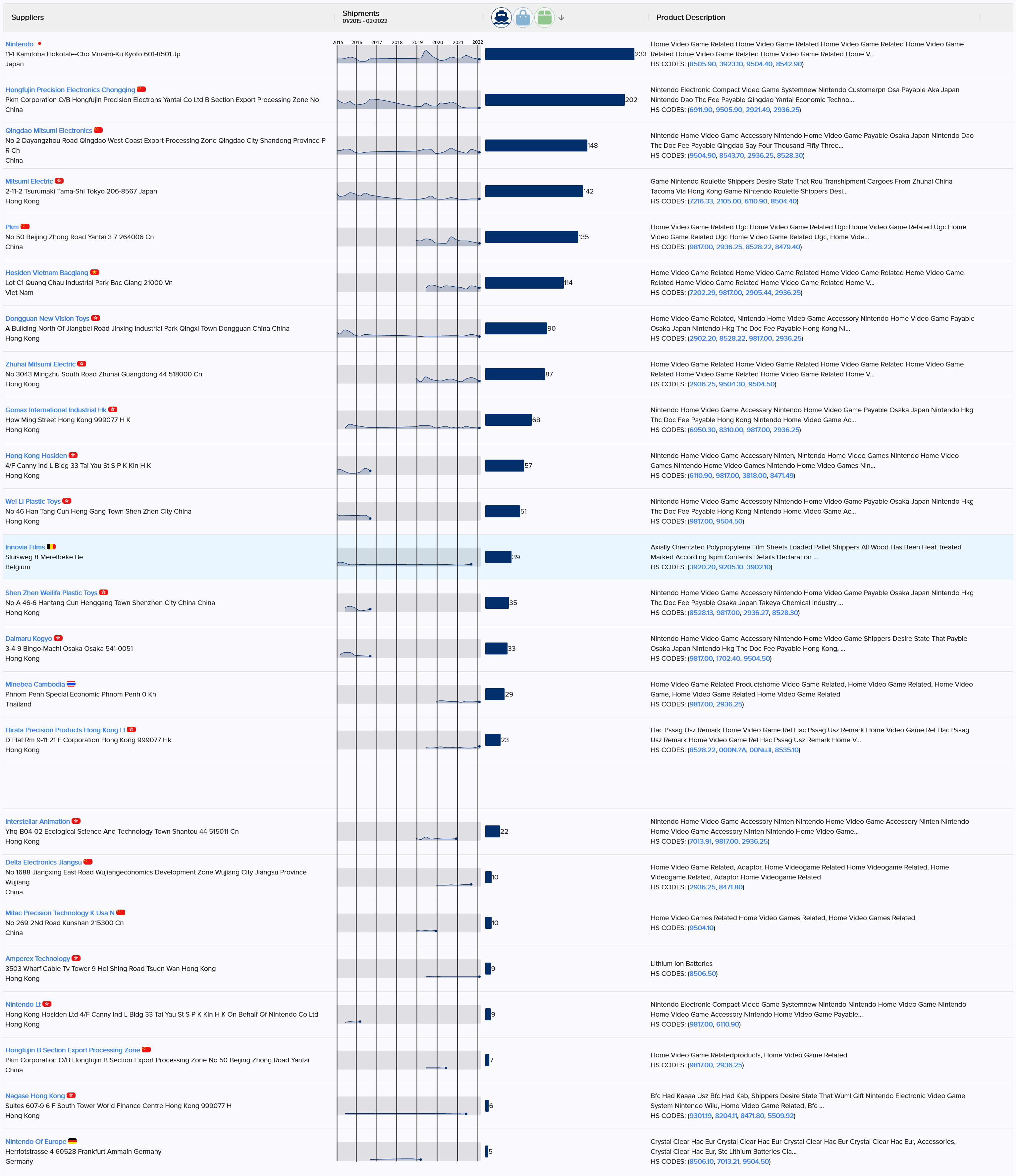
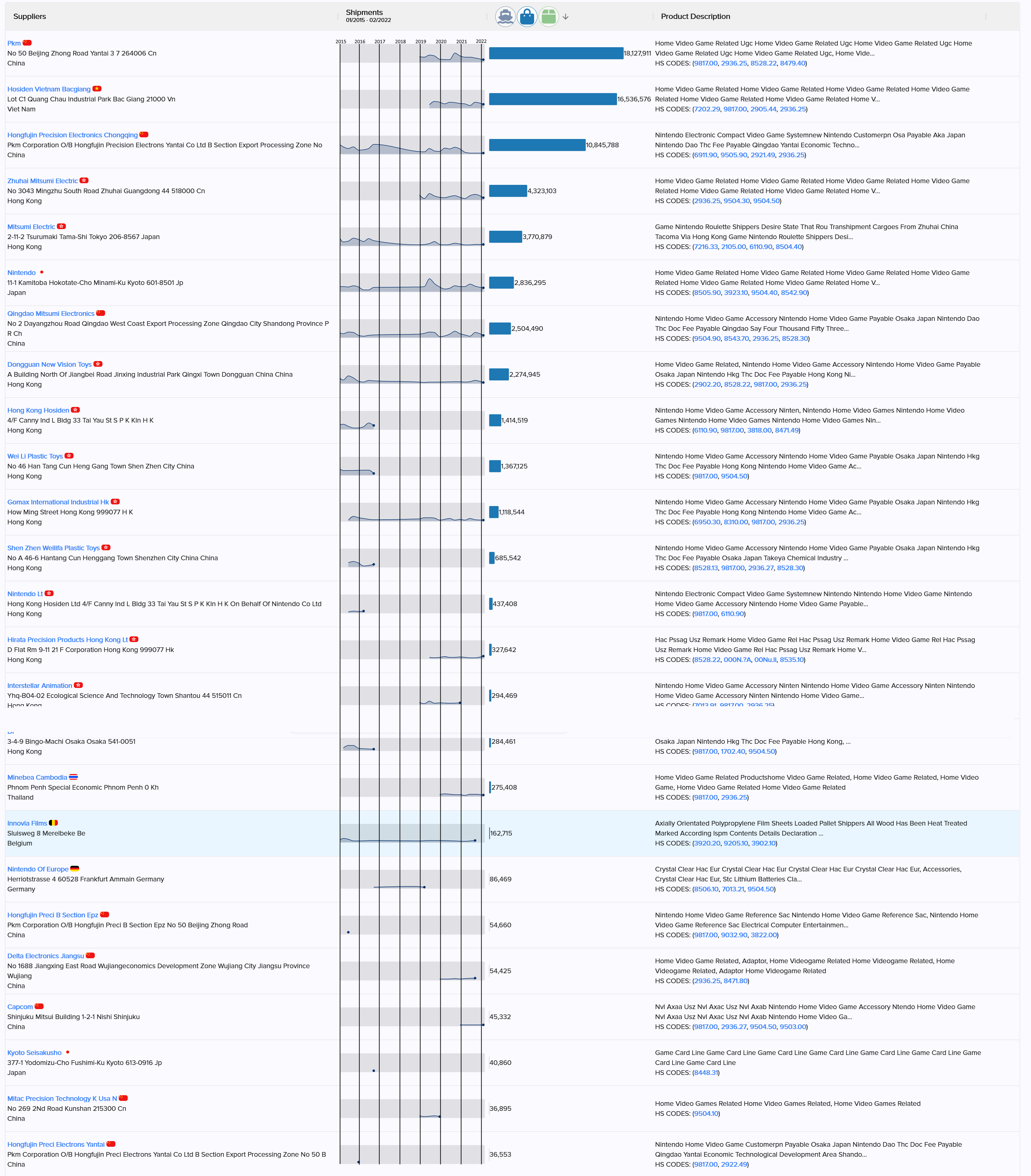
I have no idea how to glean any useful information from this but I just want to thank you for the hard work and let you know it's not being ignored.Here are some shipment records (of imports) of Nintendo of America, covering the last 7 years. (source)
I can't vouch for the accuracy of the data, as it's my first time using the specific site, but their source seems to be the official US custom records so I go with that.
The records include suppliers that manufacture different parts/modules of (current and past?) Nintendo hardware.
For example Amperex Technology seems to be the manufacturer of Switch's battery, but others are not so easy to "match" to specific hardware parts, at least for me. (I'm pretty sure Foxconn it's somewhere in there with a dif. name)
I tried looking for patterns in the graphs (hence the sloppy vertical "year" lines) correlating shipment spikes with "significant" events e.g. console launches, devkit shipments(!) etc, but it's running a bit late here so I'll leave it here for now.
I bet Nintendo of Japan's records would look even more interesting, but I don't know if those are publicly available for free, so NoA's records will have to do for now. Maybe someone can get something out of it.
For those interested, I recommend checking the records from the site itself as my screenshots are probably missing the 2nd page of the results, and that page might include a new/interesting supplier that's listed towards the end just because of sorting.
The two lists are sorted by:
- Number of sea shipments
- Weight in kg
Honestly, I don't think the former assertion is true, but it's certainly pushing the limit. There's definitely some room for a bigger chip in the Switch.my post was predicated on the idea that I think 8nm 12sm hybrid is basically impossible and any silly alternative is more likely
but as pointed out I don't really have any basis for the former assertion
Yeah I really think the size itself isn't really a problem.Honestly, I don't think the former assertion is true, but it's certainly pushing the limit. There's definitely some room for a bigger chip in the Switch.
Heat is a question of whether they can reign in the power consumption of the chip as low (or nearly, anyway) as the TX1 without tanking the performance. That's potentially the biggest obstacle, but Nvidia and Nintendo are the only ones who have a clue as to where they are on the power curve. There's a chance it's not a problem at all.Heat too, generally a wider die will be better at spreading heat. Especially if it's clocked low, I'd expect there to be less cooling needed, not more.

Lately for me it's been the latter, though that's more because of work and kids making me too tired to stay up late.A small question.
Do you play with your Nintendo Switch or you just enjoy talking about it?
I play on it some daysA small question.
Do you play with your Nintendo Switch or you just enjoy talking about it? I mean... Are you guys even going to play with your Switch Pro/2/Super/Ultra?
More towards the latter since I've recently started my job a little more than a week ago. I do try to play on my Nintendo Switch from time to time whenever I'm not too tired or busy.A small question.
Do you play with your Nintendo Switch or you just enjoy talking about it? I mean... Are you guys even going to play with your Switch Pro/2/Super/Ultra?
A small question.
Do you play with your Nintendo Switch or you just enjoy talking about it? I mean... Are you guys even going to play with your Switch Pro/2/Super/Ultra?
A small question.
Do you play with your Nintendo Switch or you just enjoy talking about it? I mean... Are you guys even going to play with your Switch Pro/2/Super/Ultra?