
- Pronouns
- He/Him
LOL
who better than Pikachu to show off your console's raw power
Detective Pikachu film version was a beaut tho. It won’t be a showcase but it should be
LOL
who better than Pikachu to show off your console's raw power
I wish it'd be an option, but it'd probably be trouble as a default. Some games change more than just visuals between modes. Like touch screen controls, or the different control modes in Pokémon Let's Go. Also depending on how BC works, forcing docked mode could result in people getting a worse frame rate in some games.@ReddDreadtheLead @oldpuck @Look over there
What are the odds of Nintendo running OG switch titles on drake as docked and then just downscaling the 1080p output to a 720p screen (when in handheld) and leaving it at 1080p when docked?
There are plenty of games with Switch and PS4 versions. This wouldn't be so dissimilar.I imagine a cross platform release for a Switch/“Switch 2” game would be a little less impressive, or they would drastically have to dress up the next gen version to make it look significantly better than its switch counterpart. We are expecting this thing to be quite a leap over the switch’s specifications, right?
Nah. GameCube users in 2006, Wii U users in 2017, easy to throw under the bus. Switch users in 2023 are carrying a bunch of buses around they can beat Nintendo with.Wait, guys, is there a timeline where Nintendo breaks internet (again?) by announcing that the Drake version of Zelda will actually release before the announced date? Like in March or April, maybe at the same time as Drake, and only later (so may 12th) for the standard Switch version.
I don't think it's likely at all but thinking about the possible reactions kind of hyped me haha
X360 original. I don't know what all they did for the PC/PS4/One versions, but they really blew things up.2 DVDs on PC?
I guess patch after patch (and maybe DLC?) the game has grown uncontrollably.
Aside: Can I ask for that anyway out of curiosity?As we've discussed before, what the "best slate" is for Drake depends heavily on how they position it, a thing we don't know
I don’t think you’re wrong, but I do think that your responding to something other than my point. My point wasn't that this narrative was true, my point was to game out multiple possible strategies. People playing Breath of the Wild on Wii U did not get a compromised experience, and people playing BotW on Switch got to experience the device's key selling point - that it was portable. If you're launching a new Switch whose USP is a generational leap in power, then you cannot do that again. Either the base Switch version and the Drake version are basically the same, or the Drake version shows off what the device can do.
Which of those is most useful to Nintendo depends on how Nintendo wants to position the hardware - but also what else they might launch with it, and we know that there are at least 9 launch year games for the device we haven't heard of. The number of known unknowns here is high.
I can tell you with 95% confidence what the CPU L1 cache miss rate for BC games running on Drake, along with the associated pipeline penalty for a miss, but not only is marketing not my strong suit, but Nintendo is going to do something unprecedented no matter what strategy they use, and they have chess pieces on the board we haven't even heard of to execute that strategy.
Fun to speculate? Yes. Clinically dangerous levels of salt required for each take? Also yes
The next generation of that game where you yell expletives at Pikachu. But now there's ML acceleration. That Pikachu learns.LOL
who better than Pikachu to show off your console's raw power
Sounds more like hopes to me. MP4 wasn’t even been shown yet, I don’t expect the marketing cycle to start soon tbh. We don’t know anything about 3D Mario. New F-Zero/Wave Race wasn’t in the talks either, maybe a GC remaster for F-Zero. For StarFox, we only know about prototyping which means nothing really, they do that all the time. Nothing about Nintendo Land, Arms, Pilotwings or a new IP either.
Sorry
The only games that are somehow rumored are DK and the MP remaster. Since we kinda expect the next Switch to launch in the first half of 2023, I don’t expect a blow-out as your list suggests. We‘re also set until May with some gaps after February. So I guess we may get 1 or 2 more titles before Zelda, and then that will be the big new thing. Everything else (Metroid, 3D Mario etc) could be considered for next Holiday season.
since star fox on SNESOr we just get a brand new Star Fox game and stop rehashing the same SF game over and over? They’ve been prototyping a new game since 2018.

gets us excited for next gen pokemon only for Game Freak to disappoint!LOL
who better than Pikachu to show off your console's raw power
Hey You! Pikachu 2!The next generation of that game where you yell expletives at Pikachu. But now there's ML acceleration. That Pikachu learns.
"OH GREAT, DISPLAY LOTTERY"
But yes, finding another provider would make the most sense unless Nintendo is going full mad-lad and just replacing the OLED model, as you say.
The circumstances of the 3DS display lottery are not nearly the same as they were, because that was caused by using 2 different types of LCD panel. Uniformity of the tech supplied by suppliers and the whole worry disappears. It’s unnecessary fear.Please, no display lottery EVER again. The New 3DS lottery with IPS panels was a nightmare and while I got a nice Hyrule edition, it still doesn't have IPS on the touch screen.
I remember I ordered and sent back units at least 3 times because I just wanted a good display, it's so ridiculous
Internet infrastructure is still pretty awful across most of Nintendo’s biggest markets, for a myriad of different reasons that have been known for the past 15-20 years already.Every game company wants to go digital only: they'll make more money and cut out the middle man. Each generation they will consider it and look at factors such as cost to produce media, consumer behavior, internet infrastructure, etc before making a decision. It's not silly entertainment, it's a business decision. But by all means, stifle discussion of something new in lieu of the same old conversations about ram amount, clock speed, thermals, and launch date.
There are games that cost more on the Switch than they did on the xbox or ps4 because cards cost more to make than blurays.
Proprietary storage costs more. There's R&D costs, finding the right partners to manufacture it, etc. If Nintendo sticks with carts and want backwards compatibility they need to design a slot that can take both kinds of carts and design a cart that is capable of delivering data at the speed that modern gaming demands. Totally do-able, but it's a lot more expensive than buying a few servers or printing out digital codes.
Not all devices provide the same profit margins to retailers or have the same revenue sources. Changing to a digital-only model would likely mean that the current profit margin model for retailers (which have been pretty static since the introduction of digital storefronts when retailers assuredly last argued for a substantial profit margin increase) would need renegotiation and consoles would require retail price adjustments to account for a higher profit margin to retailers. So higher console MSRPs.Best Buy sells tons of devices with digital storefronts. They dedicate a large part of their store to just selling apple devices. The middleman will keep middle-manning even if there's fewer plastic clamshells to line the the shelves. Not to say there's no repercussions, but Best Buy isn't going to stop selling Switch Pro Controllers.
It isHow come it's only 2.39x improvement for the same 1 GHz.. I thought the IPC for A78s is roughly 3x that of A57s. Or maybe there is something I'm not getting..

Well just like PS5 and XBS, games that require faster read speeds could be forced to be installed on the internal storage directly, at least a portion of that game that needs the fast speed, this is why 128GB is the bare minimum storage expected. 256GB is also feasible to encourage people to buy digitally.You're right. 100MB/s is a great speed for next gen gaming. Nintendo should totally use 100mb/s carts in the next switch. My arguments have been torn asunder!
And your point about Indie games is also spot on. Indie games are the only games Nintendo will be considering.
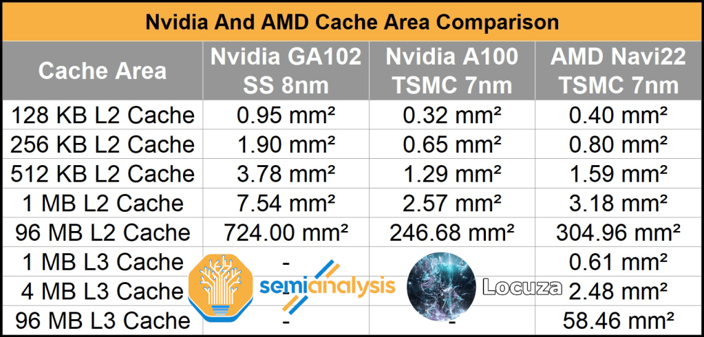
There’s nothing that really indicates that the 8N that nvidia uses can be denser than the rest of the Ampere lineup. Nvidia also doesn’t use any mobile libraries for the ampere line of GPUs, or especially ORIN which would have made it a lot smaller.
Drake has a much bigger GPU than the Steam deck Van Gogh APU, having 3 times as many shaders to it. The cache on 8nm also takes up a significantly larger amount of die space than on the 7/6 or 5nm node.
The CPU is smaller so it’s fine, x86 are way larger than ARM.
However, the thing is supposed to have 8x16 memory controllers for 128-bit.
Then there’s the logic in this which will be way larger than the better nodes. And that takes a significant chunk of die space.
I’d posit that 8C+12SM SoC would be between 160-180mm^2.
On 7nm it should be 100-115mm^2
6nm like 93 and 99mm^2
On 5nm it should be between 70 and 80mm^2
And 4N should be like 65-65 I think?
And this is based on how ampere is and how it scales with the better nodes. For a soc like this I’d imagine using the mobile libraries would be better though.
You’re in the right direction generally and the wrong direction specifically, because my claim was a little bit of a cheat by specifying BC.Aside: Can I ask for that anyway out of curiosity?
On that topic, I'm trying to wrap my head around the power law of cache misses.
Using the TX1 and A78-as-implemented-in-Orin as an example:
TX1 has 48 KB L1 instruction/32 KB L1 data
A78-in-Orin has 64 KB L1 instruction/64 KB L1 data
Going back to the power law of cache misses, M = M0*C^(-a), a ranges from 0.3 to 0.7.
M0 is the miss rate for the baseline amount of cache. Is C an absolute amount of cache or a relative amount? Like say, if it's relative, A78 has L1I cache that is (64/48) times the TX1's amount (or, 4/3). Then M ranges from (4/3)^(-0.7)~= 0.82 to (4/3)^(-0.3)~= 0.92 times M0. That is, the A78 here has a miss rate for its L1I cache that ranges from ~82% to 92% of the TX1's L1I cache miss rate. And for L1D, we're looking at (64/32), or 2x size. Then the range is 2^-0.7~= 0.62 to 2^-0.3~= 0.81, so the A78 here has a miss rate for its L1D cache that ranges from ~62% to ~81% of the TX1's L1D cache miss rate? Or I'm heading in the wrong direction with what to plug in for C?
The next generation of that game where you yell expletives at Pikachu. But now there's ML acceleration. That Pikachu learns.
ack I didn’t answer your question! C is absolute, but the algorithm is effectively relative because you compute the cache hit rate for a baseline amount of cache.Aside: Can I ask for that anyway out of curiosity?
On that topic, I'm trying to wrap my head around the power law of cache misses.
Using the TX1 and A78-as-implemented-in-Orin as an example:
TX1 has 48 KB L1 instruction/32 KB L1 data
A78-in-Orin has 64 KB L1 instruction/64 KB L1 data
Going back to the power law of cache misses, M = M0*C^(-a), a ranges from 0.3 to 0.7.
M0 is the miss rate for the baseline amount of cache. Is C an absolute amount of cache or a relative amount? Like say, if it's relative, A78 has L1I cache that is (64/48) times the TX1's amount (or, 4/3). Then M ranges from (4/3)^(-0.7)~= 0.82 to (4/3)^(-0.3)~= 0.92 times M0. That is, the A78 here has a miss rate for its L1I cache that ranges from ~82% to 92% of the TX1's L1I cache miss rate. And for L1D, we're looking at (64/32), or 2x size. Then the range is 2^-0.7~= 0.62 to 2^-0.3~= 0.81, so the A78 here has a miss rate for its L1D cache that ranges from ~62% to ~81% of the TX1's L1D cache miss rate? Or I'm heading in the wrong direction with what to plug in for C?
No.So whats the consensus, if a Shield TV 2 gets announced does kill the hopes of getting a next Switch soon?
any shield tv would just be orinSo whats the consensus, if a Shield TV 2 gets announced does kill the hopes of getting a next Switch soon?
I agree with this completely, early on most of us were under the impression that whatever the next Switch SoC was would also be slotted in as the Nano product for Nvidia's Ai solutions. But with the announcement of the Orin Nano and its differences from Drake, it definitely feels like Nintendo might land with a chip that is more bespoke to them this time around and not shared with the Shield TV...any shield tv would just be orin
Everything in this post still applies even if Shield TV or some other product happens.So whats the consensus, if a Shield TV 2 gets announced does kill the hopes of getting a next Switch soon?
any shield tv would just be orin
If that's the case, then why does Nvidia care about running Linux on T239?I agree with this completely, early on most of us were under the impression that whatever the next Switch SoC was would also be slotted in as the Nano product for Nvidia's Ai solutions. But with the announcement of the Orin Nano and its differences from Drake, it definitely feels like Nintendo might land with a chip that is more bespoke to them this time around and not shared with the Shield TV...
The only reason I can think of is independent verification. There may or may not be an out for using this chip elsewhere, and if testing and whatnot costs them little to nothing, why not keep an option in the back pocketIf that's the case, then why does Nvidia care about running Linux on T239?
Again outside of paper specs I'm just looking at what both Nvidia and AMD have achieved on respective manufacturing processes aligned with their products released. The Ampere cards are getting transistor densities of roughly 44Mtr/mm² on Samsung's 8N and the newer PS5 Oberon Plus is getting around 40Mtr/mm² on TSMC's 6nm. All of these SoC's have various forms of memory controllers and cache logic on die, so that's not unique to Drake on Samsung's process (if that's where this chip is manufactured in the end).
But just for comparison sake based on Van Gogh being 2.4 billion transistors with a 163mm die, Nvidia could achieve a chip with roughly 3x the density in the same die space for Drake. Also we know how Nvidia achieved the higher amounts of shader cores from Turing to Ampere and it wasn't by essentially doubling the gpu size, so the amount of shader cores vs Van Gogh isn't that great of a comparison.
Edit: This TechPowerUp article on AMD's Van Gogh list the APU as having
"AMD's Van Gogh GPU uses the RDNA 2.0 architecture and is made using a 7 nm production process at TSMC. With a die size of 163 mm² and a transistor count of 2,400 million it is a small chip. Van Gogh supports DirectX 12 (Feature Level 12_1). For GPU compute applications, OpenCL version 2.0 can be used. It features 512 shading units, 32 texture mapping units and 16 ROPs. The GPU also contains 8 raytracing acceleration cores."
All of this with a transistor density of 14.7 Mtr/mm² on 7nm which probably helps in achieving higher CPU clocks and cooling, again Switch in this instance can benefit from less than max clocks for a hybrid style device.
You aren’t understanding, I’m factoring in the three times density, it would still be bigger than the APU in the steam deck. It would still be literally physically bigger than that APU. Despite being three times denser, it would still quite literally be bigger. I don’t know how I need to explain this more but it is factoring the density there’s three times what the steam deck has and it is quite literally still physically bigger.
And the reason I compared the Ampere shader count is because the comparison is to RDNA2, not Turing. It quite literally had a larger APU all things considered.
Those numbers from before aren’t pulled out of nowhere, it’s an approximate estimate based on actual things we know.
you mean slightly under based on what Kopite 7 saidOK forget comparing to Steamdeck, the full GA107 gpu is under 200mm² on the same 8nm process for 20SM's what are we discussing here...
The battery basically replaces part of the power supply in a standard console, computer or laptop. My info here is a bit rusty, so I hope I got this right.Not the subject you would expect to talk about in this thread, but I really want to ask: why does the switch not work without a battery? I'm curious about the technical aspect, and why to make this design choice.
My 3ds' battery died months ago and I had to remove it. Unfortunately I couldn't play just connecting the charger cable. And it's not easy (nor cheap) to buy an original one where I live (there's no support from Nintendo for the 3ds here). I still play on my SNES and N64, so it's not a good feeling knowing the same can happen to my switch. Of course, hardware can break. It can happen with my old consoles. But anyway, what's the reason to not work just connecting to the charger?
Does the battery come with some specific hardware that makes it unnecessary to have another one on the console itself? Make it work like those notebooks (where you remove the battery and can still use it using the charger) would substantially increase complexity/costs?
I’d posit that 8C+12SM SoC would be between 160-180mm^2.
On 7nm it should be 100-115mm^2
6nm like 93 and 99mm^2
On 5nm it should be between 70 and 80mm^2
And 4N should be like 65-65 I think?


You’re all free to expect whatever, of course, but I’d…really not expect N4.
TSMC N7/N6 is still a great node. ]
Uh, 118mm^2 for Erista, 100mm^2 for Mariko I think.What were the sizes of the Switch SoC and its shrink for comparison?
So if your upper estimates are more accurate then it definitely sounds like that at the very least if they want to keep the same form factor that TSMC’s 7nm node is the minimum they should be going with then, right?Uh, 118mm^2 for Erista, 100mm^2 for Mariko I think.
Double checked.What were the sizes of the Switch SoC and its shrink for comparison?

It doesn’t actually mean that they necessarily have to test every game, it’s not like they’re moving to some totally unrelated hardware like Xbox 360 to Xbox One.I know this question already has been discussed a lot, but what is the opinion around here on how they'll do backwards compatibility?
Completely new chip means that games need to be adapted and tested, will Nintendo do that by themselves similarly like Microsoft?
Updating games shouldn't be super time consuming, because of evolution of software (NVN2) and hardware, but then it could still be possible that quite a few Switch games aren't ready at launch for Drake.
Or do you think that they'll go a different route, like including the Tegra X1 in the new chip?
I wonder how Windows and Android does it.It doesn’t actually mean that they necessarily have to test every game, it’s not like they’re moving to some totally unrelated hardware like Xbox 360 to Xbox One.
I imagine BC will be done via a compatibility layer that gives them like 99% compatibility and some games will get updates to take advantage of the hardware.
Obviously they would do a ton of testing when developing the compatibility layer, but they wouldn’t have to test every single game.
For Android I'm not sure but on Windows the likely answer is that they just don't lol. The latter provides so many layers of abstraction anyway, to the point that one can run each application in compatibility mode back to Windows 98 I think (will double check quickly on my laptop) and see for themselves.I wonder how Windows and Android does it.
As I understand it the CPU is already directly compatible, so they don't need to worry about that. For the GPU the Maxwell instruction set is not directly compatible to ampere's so they'd need to translate those instructions at runtime.I know this question already has been discussed a lot, but what is the opinion around here on how they'll do backwards compatibility?
Completely new chip means that games need to be adapted and tested, will Nintendo do that by themselves similarly like Microsoft?
Updating games shouldn't be super time consuming, because of evolution of software (NVN2) and hardware, but then it could still be possible that quite a few Switch games aren't ready at launch for Drake.
Or do you think that they'll go a different route, like including the Tegra X1 in the new chip?
I will eat my hat if it’s TSMC N4. The iPhone 14 Pro, which is if I’m not mistaken the first and currently only shipping product on TSMC N4, came out less than two weeks ago. And Apple is still transitioning a lot of their product stack to N5P, with the upcoming M2 Pro and M2 Max SoCs generally expected to be on that second-generation TSMC 5nm node, not N4.
I just don’t see Nintendo putting a high-cost bleeding-edge node (that has yet to even make it into the non-Pro iPhone) into this thing. Forget what’s traditional for Nintendo – that’s just not the way consoles have generally worked. The equivalent would be the PS5 and Xbox Series X shipping with 5nm SoCs in 2020; neither of them did. And neither of those systems had to include a screen in the box, or three rechargeable batteries, or two wireless controllers, or…
I just don’t see it. By all accounts N4 is not cheap and it’s going to be in incredibly high demand for high-end smartphone SoCs. I just don’t think it’s realistic to expect it in a game console that has to sell for, what, $400? $450 max? in the first half of 2023.
I don’t think Nvidia is calling what would historically be the 4070 GPU the “4080 12GB” and selling it at a $400 premium to past *070s because TSMC’s most advanced process nodes are just that affordable in 2022. I don’t think Apple is for the first time putting completely different generations of chips in the iPhone and iPhone Pro because N4 is just that affordable. There’s a huge capacity crunch right now and TSMC has the industry by the balls and they know it.
You’re all free to expect whatever, of course, but I’d…really not expect N4.
TSMC N7/N6 is still a great node. It’s not ancient or “withered technology” or anything. It’s still used in high quality products that actually cost within the price range we’re expecting this thing, like the standard iPad, the Apple Watch, and – oh yeah – all the other consoles.
To add to this, considering how big the GPU and CPU are, far above our expectations and the limited clocks 8nm Samsung would have to deal with, on top of Nintendo paying the highest costs for R&D for the past several years (for Nintendo), and Nvidia wanted to secure TSMC's 5nm... I'd say it's probably more likely than Nintendo decided to make a huge die with low clocks for the sake of it on 8nm.One thing worth clarifying, the TSMC N4 process, used for the iPhone 14 Pro, isn't the same as the 4N process, used for the Nvidia 4000 series GPUs. The latter is a "customised" process for Nvidia which is rumoured to be based on N5P process. The "Xnm" names foundries give to manufacturing processes have long since diverged from reality, so Nvidia likely just wanted to call it 4N so that people would think they're on a more advanced node than AMD, even though they're likely on a basically identical process.
Secondly, the difference between N5, N5P, N4 and the confusingly named 4N doesn't really matter that much. They're all part of TSMC's 5nm family of manufacturing processes, and are largely the same process, with relatively minor differences in density, performance and power. They're made on the same manufacturing lines, and a design could probably migrate from one to another relatively easily (not that there's much point). TSMC just started calling it 4nm because it sounds better, neither N4 or 4N are actual new manufacturing processes like N5 was or like their 3nm processes will be. If Drake does use a process in the TSMC 5nm family, it would almost certainly be the 4N variant, as that's what Nvidia's using for everything else. (Also I believe the first N4 chip was the MediaTek Dimensity 9000, which was in shipping products earlier this year).
The TSMC 5nm family as a whole isn't as new, as expensive, or in as short supply as many people think. In terms of timing, the first TSMC 5nm chips arrived in products toward the end of 2020. With an early 2023 launch, that would put the 5nm family at 2 and a half years old, pretty much exactly the age that 20nm was when Switch launched, and a bit older than the 7nm family was when PS5 and XBSS/X launched. In fact, the new Switch model will be in a very similar position to the PS5/XBS, as TSMC's new 3nm process will be hitting products at around the same time as the new Switch hardware, similar to PS5/XBS launching at around the same time as the first 5nm products.
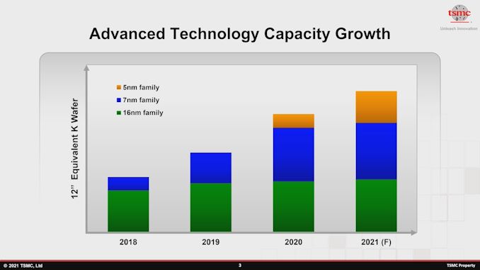
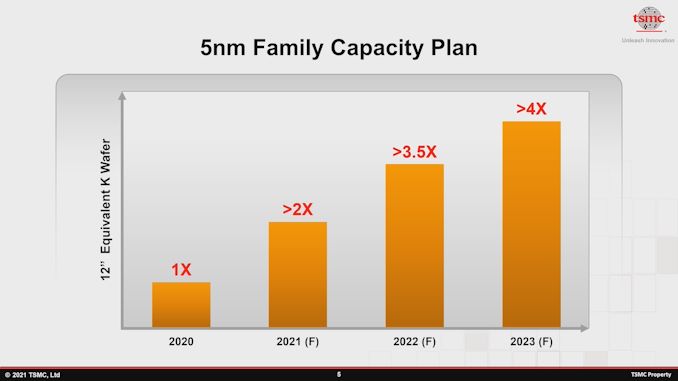
In terms of supply, TSMC's 5nm family has some of the highest wafer capacity of any manufacturing process, and accounting for transistor density may actually have the highest capacity in terms of how many chips it could produce. Take a look at these graphs provided by TSMC from this Anandtech article last year:
TSMC's plan was for the end of 2022 to have almost as much wafer capacity for their 5nm processes as their 7nm processes, likely overtaking 7nm shortly after. Obviously these were forecasts, but it's unlikely they slowed down in the past year. It's an extremely high volume manufacturing process, and we know that Nvidia has already paid TSMC a large amount of money for a signifiant allocation of it.
In terms of price, we can't say for sure what TSMC charges for its wafers, but they do split their revenue by process, so we can make some reasonable estimates about the relative cost of the wafers. From their Q2 investor report (slide 4), we know that 21% of their their revenue was from 5nm processes, vs 30% for 7nm processes. From their projections above, we would expect 5nm capacity to be about 60% of 7nm capacity in early 2022, which combined with the reported revenue, would mean their revenue per wafer is... about the same. This obviously isn't quite right, and it's possible that 5nm expansion is a bit behind schedule, or they've expanded 7nm more than expected. There's also probably a bit of a lag between capacity coming online and TSMC seeing revenue from it. Still, the revenue and capacity information provided by TSMC are inconsistent with the notion that their 5nm family is massively more expensive than 7nm on a per-wafer basis, and it would have to be massively more expensive on a per wafer basis to be more expensive on a per-chip basis.
How massively more expensive? A while back I did some rough estimates of chip costs on different processes, assuming an 8 billion transistor chip. For TSMC 6nm, that came to 112.8mm2 by my estimates, which would mean 530 would fit on a wafer, per this online calculator. With a defect rate of 0.1 per cm2, that would yield an average of 470.6 working dies per wafer. On TSMC's "4N" process, with the Ada GPUs, Nvidia is hitting between 121.1 and 125.5 million transistors per mm2. Using 121.1, that would put an 8B transistor Drake at 66.1 mm2. That would mean 916 would fit on a wafer, and with the same defect rate of 0.1, it would yield an average of 866.9 working dies per wafer.
What this means is that TSMC would have to be charging 84% more for a 5nm wafer than a 7nm wafer, just for them to be the same price per die in this case, ignoring any benefit in terms of clocks or power efficiency. Judging by the data above, it seems very unlikely to me that TSMC are charging that much for a 5nm wafer. If that was the case we'd be seeing 5nm revenue being around the same, or even overtaking 7nm revenue, which isn't the case. The 5nm family is certainly more expensive per wafer than the 7nm family, but the evidence suggests it's actually cheaper per chip, even ignoring the benefits in terms of power efficiency, which would be especially important for a device like the Switch.
Finally, the most important thing to note is that Nintendo and Nvidia aren't making this decision in 2022 with the data available to us now, they made the decision back when work started on the chip, likely in late 2019 or early 2020. That was pre-covid and pre chip shortage. Around that time Nvidia would have also been making the same decision for chips like Hopper and Ada and Grace, and in all of those cases they seem to have gone for TSMC's 5nm family. Rumours also suggest that even the entry-level chips in the Ada family (ie the RTX 4050, etc.) are being manufactured on the same N4 process, and these are likely to release at around the same time as the new Switch model. If they did choose TSMC's 5nm family for Drake, then it already would have been included in the billions of dollars they paid TSMC to reserve capacity on the process.
This isn't to say I think that Drake is certainly on the N4 process. R&D costs could have come into it with Ampere on 8nm and 7nm processes, and perhaps TSMC's 5nm capacity projections weren't quite that aggressive back in 2019/2020. But I certainly wouldn't rule N4 out, either.
This isn't to say I think that Drake is certainly on the N4 process. R&D costs could have come into it with Ampere on 8nm and 7nm processes, and perhaps TSMC's 5nm capacity projections weren't quite that aggressive back in 2019/2020. But I certainly wouldn't rule N4 out, either.
I wonder how android supports different types of GPU and not break compatibility as far back as android 4.0.For Android I'm not sure but on Windows the likely answer is that they just don't lol. The latter provides so many layers of abstraction anyway, to the point that one can run each application in compatibility mode back to Windows 98 I think (will double check quickly on my laptop) and see for themselves.
Switch 2 includes a relatively hefty, and speedy 1TB ssd. The 2024 "pro" version comes with better screen, new SOC node with better battery life, etc and comes with 2 TB drive.
128GB is a much better position than 32GB Switch in 2017, because UHD Blurays only do 100GB, where as PS4 blurays did 50GBs.You will get 128GB and you will like it.

