Thraktor
"[✄]. [✄]. [✄]. [✄]." -Microsoft
- Pronouns
- He/Him
I really don't want to get into process node posting, but either this chart's numbers are wrong, or the entire discussion where "Orin's power consumption is bad on 8nm and we need to move to at least 5nm for it to be better" has been foundationally flawed. It's not clear to me which node Orin's 8N is based on, but let's assume it's 8LPP for now. According to this chart, 8LPU offers a whopping 60% reduction in power consumption over 8LPP. That already makes it better than 5LPP! 5LPP would have 46.8% the power consumption of 10LPP, as you calculated, while 8LPU would have only 36% of 10LPP. 8LPA would be even better at 30.6% of 10LPP.
According to the other Samsung chart in this post, 8LPU is the direct evolution of 8LPP. So if T239 needed to move off 8N/8LPP to improve power consumption, why would they make the more expensive and difficult jump to branch of the family with 5LPP, even though 5LPP is less efficient than the directly available 8LPU? If 8N is actually based on 8LPU instead (which this article claims is the case), then this would make even less than zero sense, since moving from 8N/8LPU to 5LPP would actually result in a less power efficient chip than if they had just stuck with what Orin was already using.
If we believe the chart, the first possible node that would result in power savings compared to 8LPU would be 4LPP, at 25.2% of 10LPP's power consumption. Although, that's if you even trust that number, since it's based on Samsung's claim from sometime last year about a node that didn't exist then and possibly still doesn't exist today.
So I'm wondering if this chart is just totally wrong. It seems to be based entirely on Samsung's marketing claims and I don't see an indication that any testing was done to verify it.
I feel the need to state explicitly that even if the numbers are all accurate, none of this means a worse performing node is going to be used. It would just mean the 5nm rumor is wrong, and things go back to being between Samsung 8nm (though potentially a significantly better 8nm than Orin uses) and TSMC. And with that, I will try to again start ignoring process node discussions because I really just don't care.
Yeah, these node comparisons are very difficult, as there are so many variables that you can't just say X node consumes Z% less than Y node and be done with it. Diagrams like the one you quoted just muddy things further, as they're almost certainly combining measurements made in different ways at different times on different circuits at different points of the voltage curve, and trying to align them all together is a quick path to madness.
However, in the case of comparing Samsung's processes, there is one slide they have shown which is at least like-for-like across multiple manufacturing processes:
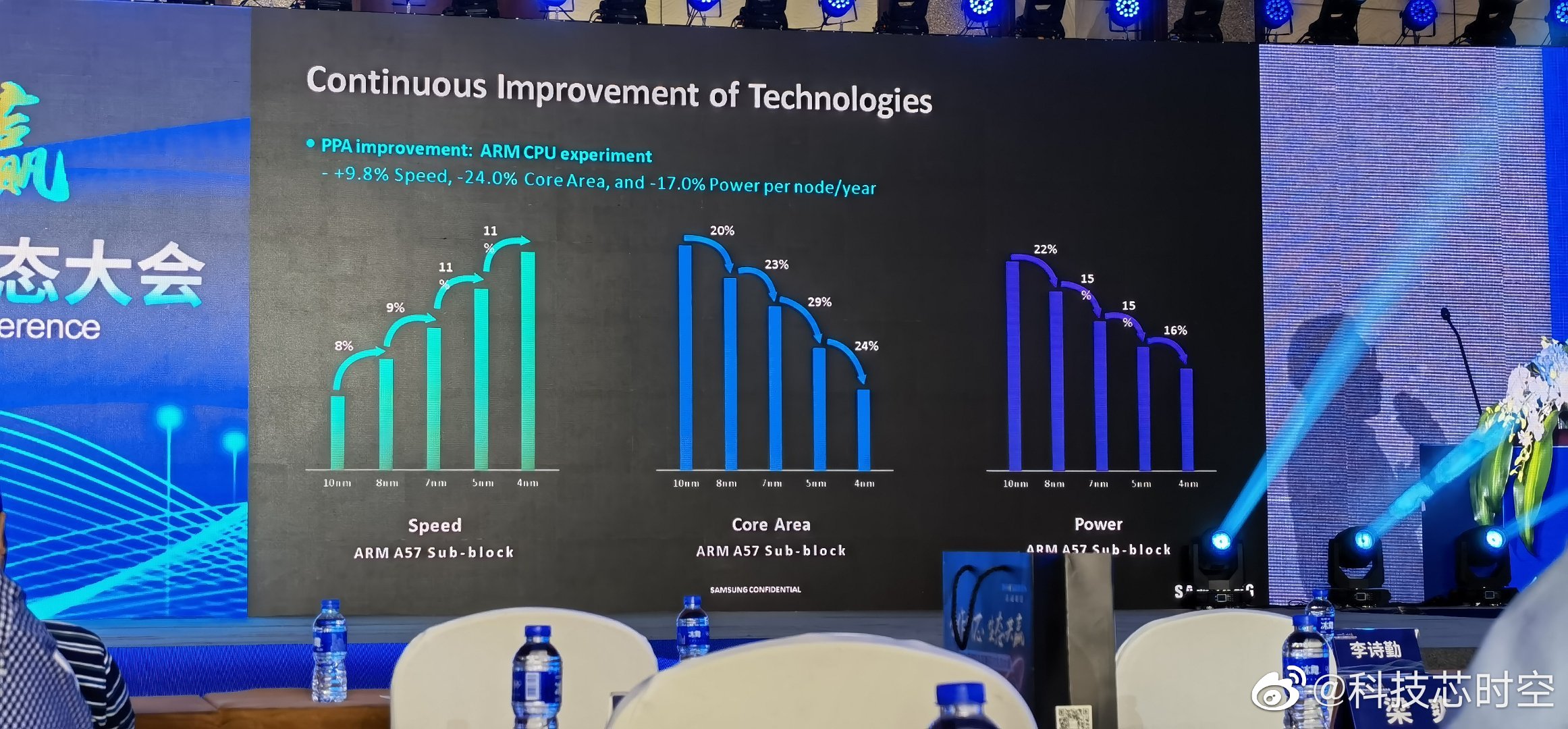
This is from a presentation in July 2021 covered by Anandtech. It's interesting because rather than the usual numbers provided completely out of context, they're specifically measuring the performance of a sub-block of the ARM A57 core. This doesn't necessarily have any relationship to the scaling we would see with T239's hardware on different nodes (aside from the co-incidence of using a sub-block from TX1's CPU), but it's at least a like-for-like comparison using a real-world CPU design. Frustratingly it doesn't show the exact processes, but it shows approximately a 30% reduction in power from Samsung's 8nm process to their 5nm process, which is about what I'd expect. It also shows about a 20% increase in clocks, presumably at ISO-power.
Again, this can't be directly extrapolated to something like T239, and the power savings can vary a lot depending on where you are on the voltage curve, but it's probably the least-worst point of reference if anyone is curious about the difference between Samsung's 8nm and 5nm foundry offerings.