I think they're just basing that on the old (2019?) figure that Nvidia gave, and aren't aware of the updated 21 billion transistor number. Nvidia haven't talked transistor numbers at all during GTC, and the most recent official number of 21 billion lines up exactly with expectations based on the process and die size (17 billion would mean a lower density process than desktop Ampere, which would be very unusual). I also don't think there are two different chips here. If anything, Orin X is just a different binning of the same Orin die (possibly a higher clocked bin, given that they've reported 254 TOPS for automotive Orin vs 200 TOPS for Orin Jetson).
Thanks. Yeah, that does make sense, and I can see why limited RT would be useful for a few or Orin's applications.
To add to this, one thing worth keeping in mind is that the GPU is quite a bit more than the two SMs on TX1, and quite a few of those blocks around and between the SMs are also the GPU, perhaps as much as doubling the size of the GPU. This is pretty important for estimating the size of a small GPU like you'd get on TX1 (or Dane), in that it's not going to scale directly with the number of SMs. There's a certain amount of logic that's going to be per-GPU, a certain amount that's per-GPC, and then the part that's per-SM. For a GPU this small, there's only going to be one GPC, so the first two are effectively static, and it's important to distinguish between those parts and the SM parts. (We've also got per-TPC on the newer architectures, but I'll bundle them into the SMs, assuming the SMs are usually a multiple of two anyway).
On the positive side, this means that you could double the number of SMs and only increase the GPU die area by (let's say) 50%. On the other hand, though, it means you can't just say "If Dane GPU has X% as many SMs as Orin, it will take up X% as much space", as there's a bunch of logic there which doesn't scale.
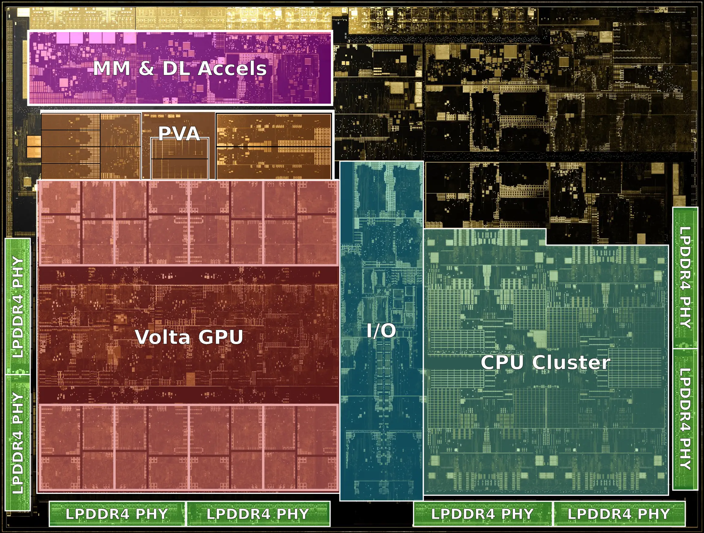
That said, we could make some inferences from the relative size of the the SMs on the different systems. The Orin die shot, as you say, is a PR shot, but probably reflects the die
as it was at the time in terms of areas well enough. As it was at the time is pretty important, though, as at the same time they said the transistor count was 17 billion and it was capable of 200 TOPS, but later updated that to 21 billion and 254 TOPS. Given it's a different shape than the final die, it's likely that the chip layout has changed a bit since then. Assuming an identical transistor density between the two, that would mean the old version of the Orin die was about 377mm2, and therefore the per-TPC die area is 8.8mm2, or 4.4mm2 per SM.
So if you assume that, from one arch to the next, the die area (not transistor count) of the per-GPU and per-GPC logic is pretty consistent, then for the same die area you'd get a 3 SM Ampere GPU in about the same die area as TX1's 2SM Maxwell GPU. Which is... not fantastic.
If you switch that around and assume that Nvidia somehow managed to keep the transistor count of GPU-level and GPC-level logic the same all the way from Maxwell to Ampere, then that logic will shrink by a factor of about 3 due to the density improvements, and you'll have more space left for the SMs. If we take the GPU of TX1 above to be 12mm2 for the SMs plus another 12mm2 for everything else, the everything else becomes 4mm2, and you're left with 20mm2, enough for 4 Ampere SMs, or 5 at a push. Even that's wildly optimistic, though, as there's obviously some transistor growth from generation to generation, and the bigger L2 cache in Orin's GPU would add considerably to that if they carried it over to Dane.
The other possibility is that other logic on the SoC outside of the GPU shrinks due to density improvements, and perhaps there's something to be gained there, or from dropping functionality which Nintendo doesn't need, but if people are also expecting an 8 core A78 CPU and a 128-bit memory bus, then those are two extra things which are going to be competing for space, so something's gotta give between these.
I've been saying for quite a while now that the most likely config for a new Switch SoC is 4 big CPU cores (ie A78), possibly with a few A55 cores, and a 4 SM GPU. That still seems the most likely outcome, and if anything the Orin reveal has solidified that, as the transistor density is the same as desktop Ampere, which means we're not getting the higher-density mobile libraries or 8LPA process improvements which would have helped them squeeze more onto Dane.
As I see it, a GPU bigger than 4 SMs is only plausible on Dane if one of three things happens:
- They use higher density mobile libraries or process improvements on 8nm. This seems very unlikely if Orin hasn't used them.
- They use a more advanced manufacturing process (eg 7nm or smaller). This seems very unlikely if the much more expensive Orin is on 8nm, and we've got reliable leaks saying it's 8nm.
- Dane is significantly bigger than the 121mm2 Tegra X1. This again seems very unlikely, and TX1 is relatively large for this type of SoC to begin with.
I don't want to rain on anyone's parade, but I see a lot of people looking at Jetson Orin NX as a basis for Dane, but if anything it's a guide for what Dane
won't do (if Dane was coming along a few months later with 1024 CUDA cores, they wouldn't have bothered releasing a Jetson with a full Orin die binned to 1024 cores). We're not going to get half of Orin at a quarter of the die size.
That said, I'd still be very exited by a Dane with 4 A78s and a 4 SM GPU based on the Orin architecture. There's a huge leap in performance and efficiency on the CPU front, and a big architectural jump on the GPU. Perhaps "only" ~2.5x as powerful in raw flops as TX1, but LPDDR5 and hopefully the much bigger caches inherited from Orin would make a big difference for any dev struggling with bandwidth, plus all the other features and improvements Ampere brings. Then, of course, the DLSS on top, and the potential for other uses of the tensor cores as ML becomes more and more common in games over the next few years.