• Hey everyone, staff have documented a list of banned content and subject matter that we feel are not consistent with site values, and don't make sense to host discussion of on Famiboards. This list (and the relevant reasoning per item) is viewable here.

StarTopic Future Nintendo Hardware & Technology Speculation & Discussion |ST| (Read the staff posts before commenting!)

Dane is derived from Orin, not Orin NX, which is a binned chip. While the NX's 25W power profile is promising... like I said earlier, Orin is a 460mm2 chip, almost 4 times bigger than OG TX1 and it will need to cut more than 1/3 of the cpu core and half the SMs to fit in a similar sized SoC.
May I note that a lot of Orin's size is using A78AE's and DLAs, and other extraneous parts due to its nature as an AI/Automotive chip?

A78AE's are FAR bigger than A78Cs (You nearly can fit 8 A78Cs into the size of 4 A78AEs)
 
So why is it ruled out that Nintendo will not go for a smaller node? I thought they were apparently not happy with the power efficiency of 8N and delayed the DSLL model (so we only got the OLED screen).
I've explained in detail the potential reasons why outside of more advanced process nodes (7 nm** and more advanced) being more expensive (here, here, here, and here).
 
I mean 8nm doesn't suck
I remember hoping that a pro system would be 12nm some time ago
haha
sure 7 or lower would be better obviously ... but I don't know... I'm thrilled this chip is not 15 years old... so a step or two back from the latest node seems good to me
 
I keep seeing this claim. Is there a source to the size difference?
NVIDIA_Orin_press_-_die_-_annotated.jpg
If Orin is indeed 460mm2, that would mean 1 A78AE is roughly 45mm2

So 1 A78AE is around 1% of the die size of Orin. and the whole block of 12 A78AEs on 8nm is around 155-156mm2.

155398-phones-news-mediatek-dimensity-1200-image1-vkvd1e08uz.jpg

That is the Dimensity 1200, a chip that while not having an official die-size revealed, looks to be at most the size of a Cheez-it which is around 24mm2.

The Dimensity has 4 A78s, and 4 A55s, and while the A55s, and GPU assembly make the chip overall smaller to fit into that "around 20-30mm2" range, the important thing is the 4 A78s.

While we have no die shot, we can extrapolate a bit of the size difference here.

Samsung 8nm that Orin is fabricated on is a tad less Dense than TSMC 7nm, the Dimensity 1200 is fabricated on TSMC 6nm which is 18% denser than 7nm.

So let's highball it and say TSMC 6nm is 30% Denser than Samsung 8nm.

That would mean a Single A78AE on TSMC 6nm, the same fabrication that has a SoC that has 4 A78s with 4 A55s and a GPU of its own.

Would eat up the majority, or all the area of the Dimensity 1200 with the "6nm A78AE" being over 30mm2

You'd need to say that TSMC 6nm is 85-95% denser than Samsung 8nm in order to fit 4 A78s into that if the A78s were the same size as the A78AEs. (At least assuming the GPU takes up the majority of space in the Dimensity like it does in some other SoCs)
 
I mean 8nm doesn't suck
I remember hoping that a pro system would be 12nm some time ago
haha
sure 7 or lower would be better obviously ... but I don't know... I'm thrilled this chip is not 15 years old... so a step or two back from the latest node seems good to me
I'm more impressed at what Nvidia accomplished at 8nm. Trading blows with a 7nm rdna2.

Now that orin is revealed, what the hell is the MX450. Crazy they will have two small GPU sizes in Turing and Ampere
 
Just catching up on the Jetson Orin info from GTC. There's not much surprising about it, with the exception of RT, but it's nice that we've got a white paper on the architecture, as I'd imagine Dane will be very similar. On the RT cores, the fact that they're there at all is a surprise, but perhaps more interesting is the choice to include half as many of them as desktop Ampere. It almost seems as if they're there for compatibility reasons, or maybe they found some limited automotive use-cases for them and decided to keep some limited functionality there. In any case, it does increase the likelihood that we see RT cores in Dane, but it reduces the expected performance of those cores even lower (from a pretty low base), so I still have low expectations of many games making extensive use of them.

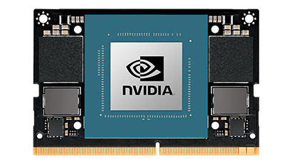
There is one thing which we can infer from the photos provided, though, which is the size (and therefore transistor density) of Orin. In particular, the Jetson AGX Orin and Jetson Orin NX pages both provide nice head-on photos of the boards, which makes calculating the die size easy. As these don't show the actual bare die (just a grey rectangle with the Nvidia logo), I also used the photo in this press release, which shows an actual bare die, but is lower resolution and at an awkward angle.

Using each of the three photos, the calculation in each case comes to a 22.1mm x 20.8mm die (+- about 0.1mm), for a die size of approx 460mm2. This tells us a few things:
  1. The Jetson Orin NX chip is the full Orin die, just binned with parts disabled. This is as I would have expected, but good to get confirmation.
  2. The Orin die has a density of approx 45.6 million transistors per mm2, assuming 21 billion transistors is still correct.
  3. This is in line with the density of GA102, GA104, etc., so it's likely using an identical 8N manufacturing process, and isn't using higher-density mobile libraries.
So, if we're to assume about a 100mm2 die size for Dane, a transistor count of about 4.5 billion seems likely. This compares to 2 billion transistors for the TX1/Mariko chips used in existing Switch models.

I have to find the video but there's one of a engineer I believe talking about RT being used in automotive guidance systems to help with object detection.
Yes, but the NX is a binned Orin, so it doesn't have to worry about die size (which is 460mm2 for both). It also uses 25W at max clocks which is roughly twice what OG Switch used docked (max 18W with 4W being from charging IIRC).

Die size affects how many SoCs they can manufacture per wafer. Using this site just for a quick example (not necessarily accurate), going from 11x11mm (121mm2, roughly OG TX1) to 12x12mm (144mm2) meant a ~17% drop in production (492 -> 409). So keeping it small is part of the balancing act.

Orin AGX makes me confident that 4 A78 + 4 SM fits in a chip around a OG TX1 size (a little more than 1/4 of Orin's size) before cutting unnecessary things and Orin NX TDP makes me confident that they could use max clock for those. I don't have the knowledge about how much more they could pack within a TX1-like size and I'm not betting on Nintendo going for a significant bigger chip nor increasing docked wattage. CPU seems like a bigger priority as well, since Nintendo is more about gameplay than pushing graphics and that will facilitate 3rd party ports more (since GPU work is much easier to scale). And thus, my previous comment.

It might be to soon to say definitive what size chip or configuration Dane will have, but we have to factor in all of the automotive specific hardware that would be removed from the design and the end goal being DLSS... So realistically 4SM vs 8SM and how high would 4SM need to be clocked in order to make that design work?
 
NVIDIA_Orin_press_-_die_-_annotated.jpg
If Orin is indeed 460mm2, that would mean 1 A78AE is roughly 45mm2

So 1 A78AE is around 1% of the die size of Orin. and the whole block of 12 A78AEs on 8nm is around 155-156mm2.

155398-phones-news-mediatek-dimensity-1200-image1-vkvd1e08uz.jpg

That is the Dimensity 1200, a chip that while not having an official die-size revealed, looks to be at most the size of a Cheez-it which is around 24mm2.

The Dimensity has 4 A78s, and 4 A55s, and while the A55s, and GPU assembly make the chip overall smaller to fit into that "around 20-30mm2" range, the important thing is the 4 A78s.

While we have no die shot, we can extrapolate a bit of the size difference here.

Samsung 8nm that Orin is fabricated on is a tad less Dense than TSMC 7nm, the Dimensity 1200 is fabricated on TSMC 6nm which is 18% denser than 7nm.

So let's highball it and say TSMC 6nm is 30% Denser than Samsung 8nm.

That would mean a Single A78AE on TSMC 6nm, the same fabrication that has a SoC that has 4 A78s with 4 A55s and a GPU of its own.

Would eat up the majority, or all the area of the Dimensity 1200 with the "6nm A78AE" being over 30mm2

You'd need to say that TSMC 6nm is 85-95% denser than Samsung 8nm in order to fit 4 A78s into that if the A78s were the same size as the A78AEs. (At least assuming the GPU takes up the majority of space in the Dimensity like it does in some other SoCs)
I completely forgot we had a die shot of Orin.

But you made a mistake in the calc. I can't pixel count right now, but visually the A78AE is roughly 10% of the width and 10% of the height, making it 1% of the area. The Orin is roughly 22mm x 22mm = 460mm2 of area, so the A78AE is roughly 2.2mm x 2.2mm = 4.6mm2, not 45.

With that said, looking at the die shot without pixel counting, 8 SM should be 70~90 mm2, so my - layman - guess would be they can fit 8 A78AE + 6 SM, MAYBE 8 A78C + 8 SM.
 
NVIDIA_Orin_press_-_die_-_annotated.jpg
If Orin is indeed 460mm2, that would mean 1 A78AE is roughly 45mm2

So 1 A78AE is around 1% of the die size of Orin. and the whole block of 12 A78AEs on 8nm is around 155-156mm2.

155398-phones-news-mediatek-dimensity-1200-image1-vkvd1e08uz.jpg

That is the Dimensity 1200, a chip that while not having an official die-size revealed, looks to be at most the size of a Cheez-it which is around 24mm2.

The Dimensity has 4 A78s, and 4 A55s, and while the A55s, and GPU assembly make the chip overall smaller to fit into that "around 20-30mm2" range, the important thing is the 4 A78s.

While we have no die shot, we can extrapolate a bit of the size difference here.

Samsung 8nm that Orin is fabricated on is a tad less Dense than TSMC 7nm, the Dimensity 1200 is fabricated on TSMC 6nm which is 18% denser than 7nm.

So let's highball it and say TSMC 6nm is 30% Denser than Samsung 8nm.

That would mean a Single A78AE on TSMC 6nm, the same fabrication that has a SoC that has 4 A78s with 4 A55s and a GPU of its own.

Would eat up the majority, or all the area of the Dimensity 1200 with the "6nm A78AE" being over 30mm2

You'd need to say that TSMC 6nm is 85-95% denser than Samsung 8nm in order to fit 4 A78s into that if the A78s were the same size as the A78AEs. (At least assuming the GPU takes up the majority of space in the Dimensity like it does in some other SoCs)
I have no idea how you reached that estimated area for a single A78AE core. My rough estimate working from the whole image being 21mmx21mm is 5.75mm² for a single core.

Granted this is just me looking at the image on my phone and estimating the whole CPU block to be ~40% of the width and ~33% of the height of the image but I can't imagine I'm all that far off, certainly not far enough off that it's actually 45mm².
 
0
It might be to soon to say definitive what size chip or configuration Dane will have, but we have to factor in all of the automotive specific hardware that would be removed from the design and the end goal being DLSS... So realistically 4SM vs 8SM and how high would 4SM need to be clocked in order to make that design work?
given that RT seems to "work" (however much that means), we're probably looking towards a higher SM count
 
0
Now that orin is revealed, what the hell is the MX450. Crazy they will have two small GPU sizes in Turing and Ampere
*MX550(Unless Nvidia brands it as RTX 3030). It's probably going to be half/third of the GA107 die. Considering the MX line is their answer to whatever the strongest iGPU at the time is, I think they will aim at close to GTX 1650 performance at 28.5W.
 
Not a single source has said they were unhappy with 8nm.
Isn't 8 the current at the moment? With 7 being bleeding edge and 5 being the next big thing? Surely we don't expect the next hardware to be bleeding edge.
 
*MX550(Unless Nvidia brands it as RTX 3030). It's probably going to be half/third of the GA107 die. Considering the MX line is their answer to whatever the strongest iGPU at the time is, I think they will aim at close to GTX 1650 performance at 28.5W.
so will it have RT cores and tensor cores? given there's no non-tensor Ampere, it sounds likely. maybe the MX550 is just a laptop version of Orin NX

Isn't 8 the current at the moment? With 7 being bleeding edge and 5 being the next big thing? Surely we don't expect the next hardware to be bleeding edge.
no, 8nm is old. it's just a better 10nm. 7nm is passe now (PS5 and Series use it, Ryzen use it, RDNA1 and 2 use it, etc). 5nm is already in products and will see more products early next year. late 2022, we might see 3nm products
 
I completely forgot we had a die shot of Orin.

But you made a mistake in the calc. I can't pixel count right now, but visually the A78AE is roughly 10% of the width and 10% of the height, making it 1% of the area. The Orin is roughly 22mm x 22mm = 460mm2 of area, so the A78AE is roughly 2.2mm x 2.2mm = 4.6mm2, not 45.

With that said, looking at the die shot without pixel counting, 8 SM should be 70~90 mm2, so my - layman - guess would be they can fit 8 A78AE + 6 SM, MAYBE 8 A78C + 8 SM.
So I was bored and was playing around with a new app I got on my iPad...

qOZyxEr.jpg


Basically just scaled the die shot to come out to ~460mm2, then got the rest from there, about ~4mm2 for the A78AEs (so of course ~48mm2 for the x12 cluster of them). Course it's all an in exact science based off a jpeg, like depending how it was cropped and how they're counting the size would mess with all those measurements.
 
What GPU do you have?

It is more likely that the 2.6FLOP/Stronger than 1050T-Weaker than GTX 1650 number is the native processing power Dane would have (1660 Super after DLSS performance, Around 2070 after DLSS Ultra Performance) considering the full "Potential" 3TFLOP number requires high levels of optimization using the double FP16 that Orin/Dane has vs Ampere.

GTX 1650 Super
 
So I was bored and was playing around with a new app I got on my iPad...

qOZyxEr.jpg


Basically just scaled the die shot to come out to ~460mm2, then got the rest from there, about ~4mm2 for the A78AEs (so of course ~48mm2 for the x12 cluster of them). Course it's all an in exact science based off a jpeg, like depending how it was cropped and how they're counting the size would mess with all those measurements.
Well for one Orin is actually a square based on the Orin NX
jetson-orin-nx-webpage-module-all-1cC-T.png

70mm by 45mm for the whole thing.
Maybe try plugging in that into your app to figure out how big the main Orin die is?

If so then we could actually figure out how big/small the full Orin Die as Orin NX is a binned Orin Die (so Orin proper is the same size).

Either way, Orin NX is quite tiny for what it's packing, and even if the A78AE's are only marginanlly bigger (they are bigger as they have some sort of extra logic for AI/Auto), cutting off 4 Cores slashes it down to 24mm2 for the A78AE's if your Orin-Dieshot number is accurate (Will have to check it against Orin NX's proper dimensions).

So 8 A78C's would likely be 20-22mm2.

And then cut the GPU die size in half (how big is the GPU there?)

With Orin NX's image and exact measurements, Orin's Dieshot (As Orin NX has the same die), and that app, we could actually figure out how much space 8SMs, and 8 A78C's would take up.

Seriously though, Orin NX is small enough to be Dane literally board size-wise if they tweaked the internals more than a plug-in solution as Orin NX has most of what is needed for a system.
 
Apologies if its been said in previous pages, but I assume nothing has changed on the front that the "Dane" Switch is still expected to be releasing between next holiday->early 2023?
 
Apologies if its been said in previous pages, but I assume nothing has changed on the front that the "Dane" Switch is still expected to be releasing between next holiday->early 2023?
Nothing really notifying much change to my knowledge no.
 
late 2022, we might see 3nm products
I don't think there are going to be any late 2022 products using 3 nm** chips, considering that TSMC said that 3 nm** wafers won't be shipped until Q1 2023, and Samsung's 3GAE process node won't start mass manufacturing until EoY (End of Year) 2022, which seems to only be available for Samsung, and Samsung's 3GAP process node won't start mass manufacturing until EoY 2023.

** → a marketing nomenclature used by all foundry companies
 
0
The interesting look is at how much Nintendo has already modified the original Switch motherboard to accommodate the OLED revamp...
1633007988328-png.277764
I think it's the daughterboard, not the motherboard, that's heavily modified. Going by IFixIt's teardown of the OLED model and the Nintendo Switch, the OLED model's motherboard still looks quite similar to the Nintendo Switch's motherboard.

OLED model:
SwitchOLED_91e.jpg

SwitchOLED_85e.jpg


Nintendo Switch:
sp3tJVWmQFybssun.huge

MiW2IHeJGIdCRJZQ.huge
And, as they mentioned, the thermal management shrank a fair bit. Even to the naked eye, you can see smaller fans and heat pipes.
 
And, as they mentioned, the thermal management shrank a fair bit. Even to the naked eye, you can see smaller fans and heat pipes.
To be fair, the Nintendo Switch's fan and copper heat pipe was complete overkill for the Tegra X1+, considering how much more power efficient the Tegra X1+ is compared to the Tegra X1.
 
I suppose I’ll link this post again for the A78 CPU cores likely space to take up.

 
0
it's very unlikely Dane is gonna come close to the 1650S
I was never saying that it would come close to the 1650S Natively XD.

At best it would get up to the 1650 Non-Super Natively.
But that would pretty much be bare-metalling it with the Doubling of FP16 optimization.

2.6 Effective TFLOPs are in the lower end range assuming a 30% boost from the L1 and L2 Cache increase.

It can go up to 3TFLOPs at the peak of optimization which is around the GTX 1650 Non-Super (Laptop)

Then add DLSS on top of that which can be accepted as a 2X boost on average for DLSS performance (4X Upscale), for 5.2 TFLOPs to 6TFLOPs.

Then add whatever multiplier DLSS Ultra Performance would bring (IMHO, it would be around a 3x boost as it is a 9X multiplier which is more than double the upscaling done for 4X, but it tapers off due to CPU overhead)
 
Although the DLSS model* probably won't be heavily affected by the global chip shortage as far as the SoC's concerned due to Dane probably being a small die, I found Yahoo Finance's interview with Jensen Huang interesting.
"I think that through the next year, demand is going to far exceed supply. We don't have any magic bullets in navigating the supply chain," Huang told Yahoo Finance Live on Wednesday.

"We have the support of our suppliers. We're fortunate that we're multi-sourced and that our supply chain is diverse and our company is quite large so we have the support of a large ecosystem around us," he added.
While Huang says the chip shortage will eventually subside, he doesn't think the level of demand we're seeing is transitory. Instead, he says it's here to stay.

"People are starting to build more and more home workstations because their home is now their office," Huang said. "And when they're at home they prefer to have a permanent system, and so desktop computers are doing incredibly well."

People are also spending more time gaming, he said, leading to more people trying to get their hands on Nvidia’s high-end graphics cards.

"I think these are permanent conditions, and we're going to see new computers being built for quite a while. People are building home offices, and you could see all of the implications," Huang said.
 
0
That interview is looking for any reason that people buy GPUs except crypto-mining, the reason the majority of people are buying consumer GPUs for nowadays. I almost feel bad for him, having to work so hard to ignore the negative association to crypto.
To be fair, the Nintendo Switch's fan and copper heat pipe was complete overkill for the Tegra X1+, considering how much more power efficient the Tegra X1+ is compared to the Tegra X1.
It was slight overkill even for Erista, if we take iFixit at their word. Which is why I was thinking 15W TDP is the moderate level of power consumption Nintendo might target for a new chip, but couldn't go much higher than 20W at the absolute maximum.
 
0
@NateDrake This is kind of random, but have you heard anything from devs about the CPU for the dane? Are they A78c or a78ae? A78c is optimized for mobile gaming and smaller althsn the a78ae in the Orion NX 🤔
 
Last edited:
Well for one Orin is actually a square based on the Orin NX
jetson-orin-nx-webpage-module-all-1cC-T.png

70mm by 45mm for the whole thing.
Maybe try plugging in that into your app to figure out how big the main Orin die is?

If so then we could actually figure out how big/small the full Orin Die as Orin NX is a binned Orin Die (so Orin proper is the same size).

Either way, Orin NX is quite tiny for what it's packing, and even if the A78AE's are only marginanlly bigger (they are bigger as they have some sort of extra logic for AI/Auto), cutting off 4 Cores slashes it down to 24mm2 for the A78AE's if your Orin-Dieshot number is accurate (Will have to check it against Orin NX's proper dimensions).

So 8 A78C's would likely be 20-22mm2.

And then cut the GPU die size in half (how big is the GPU there?)

With Orin NX's image and exact measurements, Orin's Dieshot (As Orin NX has the same die), and that app, we could actually figure out how much space 8SMs, and 8 A78C's would take up.

Seriously though, Orin NX is small enough to be Dane literally board size-wise if they tweaked the internals more than a plug-in solution as Orin NX has most of what is needed for a system.
I just realized that annotated image is based off this off angle render/press image from however long back, late 2019 from a quick search.

y8XJ1JQ.jpg


I don't know if it'd be that useful trying to use that to figure out sizes of things considering the possible changes since then along with however they decide to show crap on rendered promo images.
 
So I was bored and was playing around with a new app I got on my iPad...

qOZyxEr.jpg


Basically just scaled the die shot to come out to ~460mm2, then got the rest from there, about ~4mm2 for the A78AEs (so of course ~48mm2 for the x12 cluster of them). Course it's all an in exact science based off a jpeg, like depending how it was cropped and how they're counting the size would mess with all those measurements.
It gives me bad memories of the old threads where we did the same work with Xavier.

At the end, Nvidia still have 15W to find in order to make a NX configuration work on a custom chip.
 
0
I just realized that annotated image is based off this off angle render/press image from however long back, late 2019 from a quick search.

I don't know if it'd be that useful trying to use that to figure out sizes of things considering the possible changes since then along with however they decide to show crap on rendered promo images.
Yeah, we can't trust at all that's the real Orin in 2019 nor that it didn't change significantly in those 2 years.

But just for fun and for me to have some ballpark - which should be taken with a grain of salt - let's make several assumptions:
  • That's the real Orin, not some blueprint put together for the press release which doesn't reflect the real chip.
  • Things didn't change in size since 2019 or at least they can revert to 2019 size if needed.
  • The SoC is fully displayed in width but it's cropped at the bottom (The GPU IS cropped in the die shot, so at least this part is correct)
Then:
2000 pixels ~= 22mm, so 1 pixel ~= 0.011mm,
8 A78AE ~= 695 x 309 pixels ~= (695 x 0.011) x (309 x 0.011) ~= 26mm2
Top half of the GPU ~= 865 x 592 pixels ~= (865 x 0.011) x (592 x 0.011) ~= 62mm2

So, in a calculation which could be completely wrong, NVidia in theory could fit 8 CPU cores and 8 SM into a TX1-sized SoC with the same process node as Orin.
 
Last edited:
Yeah, we can't trust at all that's the real Orin in 2019 nor that it didn't change significantly in those 2 years.

But just for fun and for me to have some ballpark - which should be taken with a grain of salt - let's make several assumptions:
  • That's the real Orin, not some blueprint put together for the press release which doesn't reflect the real chip.
  • Things didn't change in size since 2019 or at least they can revert to 2019 size if needed.
  • The SoC is fully displayed in width but it's cropped at the bottom (The GPU IS cropped in the die shot, so at least this part is correct)
Then:
2000 pixels ~= 22mm, so 1 pixel ~= 0.011mm,
8 A78AE ~= 695 x 309 pixels ~= (695 x 0.011) x (309 x 0.011) ~= 26mm2
Top half of the GPU ~= 865 x 592 pixels ~= (865 x 0.011) x (592 x 0.011) ~= 62mm2

So, in a calculation which could be completely wrong, NVidia in theory could fit 8 CPU cores and 8 SM into a TX1-sized SoC with the same process node as Orin.
That's wrong. Most modern SoCs have a GPU+CPU ratio that is 1/3 of the overall chip. That's true for TX1, Xavier, E990 and Apple SoCs (those that don't have an integrated 5G modem like 7 nm Kirin SoCs where the ratio is closer to 1/4). By your calculations, Dane would be 264 mm2 which is more than 2*TX1.

Dane with Orin density/power consumption would be closer to Xavier performances than Orin NX perfs on the same node. We are looking at 512 cuda cores at the size of the original TX1 with probably 2 CPU cores less.
 
Last edited:
Does the SoC really need to fit 120mm2 if they plan to use more CPU cores and more SM at a lower speed to keep heat down?

Can’t they have a 135-140mm2 SoC?
They can use a very wide 400mm2 chip. It just need to run under 10W with the actual OLED battery/cooling solution.
 
0
Does the SoC really need to fit 120mm2 if they plan to use more CPU cores and more SM at a lower speed to keep heat down?

Can’t they have a 135-140mm2 SoC?
To be frank we don't even know if it'll have the same form factor as the Switch (original or OLED) so yeah I don't think they're beholden to any one die size.

They might need something bigger or smaller, we really can't know right now.
 
0
That's wrong. Most modern SoC have a GPU+CPU ratio that is 1/3 of the overall chip. That's true for TX1, Xavier, E990 and Apple SoCs (those that don't have a integrated 5G modem like 7 nm Kirin SoCs where the ratio is closer to the 1/4). By your calculations, Dane would be 264 mm2 which is more than 2*TX1.

Dane with Orin density/power consumption would be closer to Xavier performances than Orin NX perfs on the same node. We are looking at 512 cuda cores at the size of the original TX1 with probably 2 CPU cores less.

Rather than GPU+CPU, don't you mean CUDA Cores + CPU? Because from a quick check on the TX1, the 3 rectangles containing CUDA Cores and Arm cores is roughly 31.5% and that's without any margin. I honestly can't identify the remaining components of the GPU there, so I can't say how much is the CPU+GPU percent is, but if we're only looking at CUDA Cores in the ORIN die shot, they're roughly 8x169x161 ~= 26mm2.

If we extrapolate from that 1/3 rule that would be 155~160mm2. Though does that rule really stands for smaller nodes? Don't phones SoCs have anything else integrated in the SoC which a gaming console doesn't needs to?

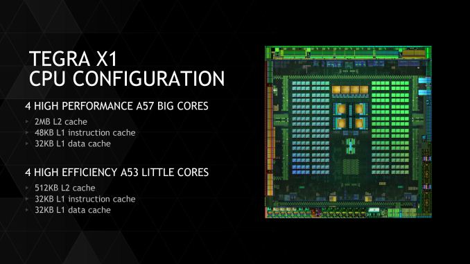
X1-CPU_575px.jpg
nvidia-20nm-tegrax1-erista-shield_tv-s_taiwan_1517a1_npw020-m3w_tm670d-a1___dieshot_segments-jpg.121116

This is a real die shot of TX1. CPU and GPU are taking a little less than 1/3 of the total chip. We don't have a real Xavier die shot but Nvidia RP 'die shots' from the pascal-turing area were more or less on point for their GPU products. That said I would expect their Xavier/Orin die shots to be slightly different from their PR die shot representations due to their nature of being SoCs with more hardware accelerated parts than GPU only chipsets.
Whoa, that's completely different from that press image. In that case, that Orin press image should be pure bullshit as well.
 
0
nvidia-20nm-tegrax1-erista-shield_tv-s_taiwan_1517a1_npw020-m3w_tm670d-a1___dieshot_segments-jpg.121116

This is a real die shot of TX1. CPU and GPU are taking a little less than 1/3 of the total chip. We don't have a real Xavier die shot but Nvidia RP 'die shots' from the pascal-turing area were more or less on point for their GPU products. That said I would expect their Xavier/Orin die shots to be slightly different from their PR die shot representations due to their nature of being SoCs with more hardware accelerated parts than GPU only chipsets.
This makes me think of Wooded Temple in Spirit Tracks, where you have to use the whirlwind to puff away the toxic clouds that are covering the place.
 
Please read this staff post before posting.

Furthermore, according to this follow-up post, all off-topic chat will be moderated.
Last edited:


Back
Top Bottom