pelusilla6
Moblin
DLSS 3.0 announced, cannot wait for HyperSwitch
afaik the Switch keeps CPU frequency consistent between docked and portable, as game logic relies upon it. GPU speeds shift since the requirements vary depending on output resolution.But I'm still guessing:
7nm TSMC
Portable: 375-450MHz GPU, ~1 GHz CPU
Docked: 850-900 MHz GPU, ~1.5-1.7 GHz CPU
Just to keep my hopes in check.
DLSS 3.0 announced, cannot wait for HyperSwitch
Hmmm... Now that I think about it, SoCs like the Snapdragon 888 (which utilizes A78 cores) and the cheaper 875 are nearly 2 years old and were manufactured under a 5nm node.
So definitely 5nm or at the very least, TSMC's 7nm could be a real possibility considering the aforementioned power efficiency concerns posted by other users ITT.
But I'm still guessing:
7nm TSMC
Portable: 375-450MHz GPU, ~1 GHz CPU
Docked: 850-900 MHz GPU, ~1.5-1.7 GHz CPU
Just to keep my hopes in check.
You know what, you're right. I saw this, thought "man, this confirms A78C" then immediately read Thraktor's comment and confused myself. This essentially confirms the C variant, yes, as base A78 has a max of 4 CPUs per cluster?I can't recall off the top of my head, but is there another feasible ARM processor that can handle a 8-core, 1-cluster configuration?
I've been thinking 7nm, because that's what Ampere is built on, but now I'm thinking 5nm since we've confirmed octo-core. A78 was built for 5nm, and Lovelace is 5nm (I believe?) and is stated to have at least started as an Ampere refresh on a smaller node.Hmmm... Now that I think about it, SoCs like the Snapdragon 888 (which utilizes A78 cores) and the cheaper 875 are nearly 2 years old and were manufactured under a 5nm node.
So definitely 5nm or at the very least, TSMC's 7nm could be a real possibility considering the aforementioned power efficiency concerns posted by other users ITT.
Other than the fact that the CPU will likely stay clocked the same (as others have pointed out) I think this is a reasonable floor, and about where my head is at too.But I'm still guessing:
7nm TSMC
Portable: 375-450MHz GPU, ~1 GHz CPU
Docked: 850-900 MHz GPU, ~1.5-1.7 GHz CPU
Just to keep my hopes in check.
afaik the Switch keeps CPU frequency consistent between docked and portable, as game logic relies upon it. GPU speeds shift since the requirements vary depending on output resolution.
The CPU is unlikely to be clocked differently between portable and docked play. They will want to keep the game logic the same when switching.

Besides the changing CPU that looks pretty reasonable.Hmmm... Now that I think about it, SoCs like the Snapdragon 888 (which utilizes A78 cores) and the cheaper 875 are nearly 2 years old and were manufactured under a 5nm node.
So definitely 5nm or at the very least, TSMC's 7nm could be a real possibility considering the aforementioned power efficiency concerns posted by other users ITT.
But I'm still guessing:
7nm TSMC
Portable: 375-450MHz GPU, ~1 GHz CPU
Docked: 850-900 MHz GPU, ~1.5-1.7 GHz CPU
Just to keep my hopes in check.
That's only for short bursts during loading, and it's done in both docked and undocked modes.
Wasn't the Switch's CPU clocked well above 1GHz anyways for certain titles like BoTW?
Only for reducing loading times.
Wasn't the Switch's CPU clocked well above 1GHz anyways for certain titles like BoTW?
So what the hell is lore.kernel.com? The Google search preview says "This is a listing of public inboxes, see the `mirror' link of each inbox for instructions on how to mirror all the data and code on this site."
Why are these inboxes public and on that site!? I don't get it.
The Switch lets games select these perf profiles per context. The "boost mode" perf is short lived and designed to be activated by games during loading screens and the like to speed up decompressing assets.
Wasn't the Switch's CPU clocked well above 1GHz anyways for certain titles like BoTW?
Those profiles are used only to accelerate load times, not during typical use. The Switch CPU is clocked to 1020mhz essentially all the time, portable or docked.
Wasn't the Switch's CPU clocked well above 1GHz anyways for certain titles like BoTW?
Real question is why than Nintendo used 1GHz instead above 2GHz? There is huge difference between 1GHz and 2GHz.
Nintendo could easily push Switch A57 to run at least at 1.2GHz or 1.3GHz, but they didnt, they usually going with more lower clocks than device could run at.
I am willing to bet that Drake will not have 2GHz CPU clock (especially if it's really 8-core CPU).
Like I wrote, regardless of node I dont see Nintendo running 2GHz or above 2GHz with Drake hardware.
We talking about mobile devices that should use those clocks all the time (for 8 cores), while in same time worrying about heating and battery life,
and Nintendo usually don't like to push clocks even hardware could run higher clocks.
You’re comparing apples to oranges here. You’re comparing the first iteration of arm’s new design, which was the A57 that supported 64-bit instruction sets to the eighth generation of CPUs the arm has which support the 64-bit instruction, and the latter is on a much superior node. On top of that you’re comparing a CPU who is designed to not clock beyond 2.1 GHz to a CPU who is designed to clock no higher than 3.3 GHz. The comparison was already flawed to begin with. Yes, they are both arm-based cores, however the A57 is very ancient at this point and as soon as you start clocking it higher than its max or close to its max, You start wasting a lot of energy, you introduce throttling, a lot of heat, etc.Thats my point, because heating and power consumption/battery life they didnt run 2GHz or above,
but they could definitely run CPU above 1GHz (for instance 1.2-1.3GHz) without big difference.
Hack scene clocked Switch CPU even at 1.8GHz and Switch was used regularly and was working without problems,
yes little higher heating and less battery life but it was working without problems.
Like I wrote Nintendo usually going with lower clocks than device could run at,
point that Drake could run 8-core CPU at 2GHz doesnt mean automatically that Nintendo will do that.
There is a boost mode that maxed out the CPU and brought the GPU to extremely low performance to help loading games since the CPU is used in decompression. That mode would is the same if you had the Switch docked or mobile as well. For gameplay the CPU clocks never change change between playstyle.
Wasn't the Switch's CPU clocked well above 1GHz anyways for certain titles like BoTW?
It's less about the specs changing since February and more about what was in the leak not necessarily having been up to date, between the lack of reliable date information, and the fact that it was a certain branch of the repository where it's not likely active development was happening directly.Do you mean the codename itself has changed or is now referring to something else? That seems extremely unlikely.
Could the specs of T239 have changed since February? Maybe, but that's also fairly unlikely considering how far along it seemingly was. But possible.
4 nm?I've been thinking 7nm, because that's what Ampere is built on, but now I'm thinking 5nm since we've confirmed octo-core. A78 was built for 5nm, and Lovelace is 5nm (I believe?) and is stated to have at least started as an Ampere refresh on a smaller node.
Other than the fact that the CPU will likely stay clocked the same (as others have pointed out) I think this is a reasonable floor, and about where my head is at too.

kernel.org is the website used to coordinate the development of the Linux kernel, which is open source. Because of the nature of that - lots of companies collaborating on a shared, public project, or even some individual developers who are funded by multiple companies - there is a mailing list that is Quite Old, and very very busy, the Linux Kernel Mailing List, or LKML for short. LKML got so busty eventually you had to bust out sub mailing lists for people to coordinate work that then gets pushed to LKML. lore.kernel.org is the archive off all those emails, so that they're searchable, because actually subscribing to the maillist is an easy way to destroy your inbox.So what the hell is lore.kernel.com? The Google search preview says "This is a listing of public inboxes, see the `mirror' link of each inbox for instructions on how to mirror all the data and code on this site."
Why are these inboxes public and on that site!? I don't get it.
Not necessarily.Kinda sounds like DLSS3 will require an Ada GPU?
Since DLSS 3 builds on top of DLSS 2 integrations, game developers can quickly enable it in existing titles that already support DLSS 2 or NVIDIA Streamline.
Based on this keynote it sounds like much of what DLSS3 does requires the new dedicated hardware in Ada GPUs.Not necessarily.
NVIDIA Introduces DLSS 3 With Breakthrough AI-Powered Frame Generation for up to 4x Performance
DLSS 3 Generates Entire Frames in Real Time With AI, Benefiting GPU- and CPU-Limited Games and Apps...www.globenewswire.com
"Powered by new fourth-generation Tensor Cores and a new Optical Flow Accelerator on GeForce RTX 40 Series GPUs, DLSS 3 is the latest iteration of the company’s critically acclaimed Deep Learning Super Sampling technology and introduces a new capability called Optical Multi Frame Generation."
Kinda sounds like DLSS3 will require an Ada GPU?
Doesn't seem like it requires native 4k frames? Just old and new frame data.Waiting for a better technical breakdown, but it looks like the big feature is the generation of new frames from old frame data, and that it uses natively rendered 4k frames to do it? In which case, you'd need a machine capable of doing native 4k at, say, 30fps, and then use this to get to 60 fps. Not sure it would apply to the Switch anyway
I'm assuming it needs to use native res. frames because it wouldn't be capable of doing both DLSS upscaling and then frame interpolation at the same time?Waiting for a better technical breakdown, but it looks like the big feature is the generation of new frames from old frame data, and that it uses natively rendered 4k frames to do it? In which case, you'd need a machine capable of doing native 4k at, say, 30fps, and then use this to get to 60 fps. Not sure it would apply to the Switch anyway
Kinda sounds like DLSS3 will require an Ada GPU?
Or, Nintendo dropped NVIDIA after the recent controversy and NVIDIA wanted to get a return on their R&D by releasing a product that uses T239

NVIDIA Unveils DRIVE Thor — Centralized Car Computer Unifying Cluster, Infotainment, Automated Driving, and Parking in a Single, Cost-Saving System
Wielding 2,000 Teraflops of Performance, Platform Integrates Next-Gen GPU and Transformer Engine to Support AI Workloads for Safe and Secure Autonomous...
 developer.nvidia.com
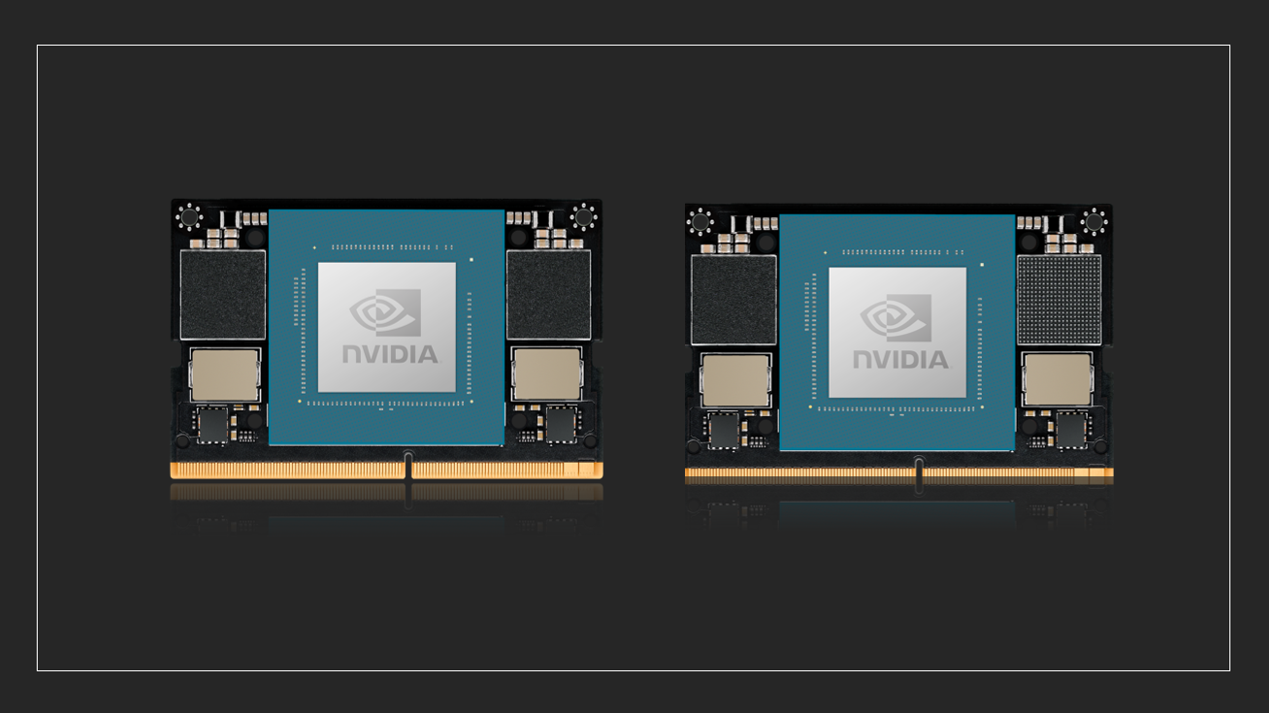
| Jetson Orin Nano 4GB | Jetson Orin Nano 8GB | |
| AI Performance | 20 Sparse TOPs | 10 Dense TOPs | 40 Sparse TOPs | 20 Dense TOPs |
| GPU | 512-core NVIDIA Ampere Architecture GPU with 16 Tensor Cores | 1024-core NVIDIA Ampere Architecture GPU with 32 Tensor Cores |
| GPU Max Frequency | 625 MHz | |
| CPU | 6-core Arm Cortex-A78AE v8.2 64-bit CPU 1.5 MB L2 + 4 MB L3 | |
| CPU Max Frequency | 1.5 GHz | |
| Memory | 4GB 64-bit LPDDR5 34 GB/s | 8GB 128-bit LPDDR5 68 GB/s |
| Storage | – (Supports external NVMe) | |
| Video Encode | 1080p30 supported by 1-2 CPU cores | |
| Video Decode | 1x 4K60 (H.265) | 2x 4K30 (H.265) | 5x 1080p60 (H.265) | 11x 1080p30 (H.265) | |
| Camera | Up to 4 cameras (8 through virtual channels*) 8 lanes MIPI CSI-2 D-PHY 2.1 (up to 20 Gbps) | |
| PCIe | 1 x4 + 3 x1 (PCIe Gen3, Root Port, & Endpoint) | |
| USB | 3x USB 3.2 Gen2 (10 Gbps) 3x USB 2.0 | |
| Networking | 1x GbE | |
| Display | 1x 4K30 multimode DisplayPort 1.2 (+MST)/e DisplayPort 1.4/HDMI 1.4* | |
| Other I/O | 3x UART, 2x SPI, 2x I2S, 4x I2C, 1x CAN, DMIC and DSPK, PWM, GPIOs | |
| Power | 5W – 10W | 7W – 15W |
| Mechanical | 69.6 mm x 45 mm 260-pin SO-DIMM connector | |
| Price | $199† | $299† |
I dunno, did they make a Shield with a Xavier chip? This also makes mention of T194 in the code sample, or is that just me reading too much into it?
I think T239 being used for a Jetson devkit is unlikely, considering Nvidia recently announced Jetson Orin Nano.It could be a Shield product, or Jetson (although that would have some overlap with Jetson Orin NX in performance), or it could be a third party product, like an Android tablet or Chromebook or whatever. Hard to tell, but they definitely expect to use this in non-Nintendo products.
developer.nvidia.com
Hey OldPuck, it's me again.
Oh hey, Anonymous Lurker, how is it going?
Any idea why there's such a large range for power consumption for these? I guess the amount they throttle?Solving Entry-Level Edge AI Challenges with NVIDIA Jetson Orin Nano | NVIDIA Technical Blog
NVIDIA Jetson Orin Nano series system-on-modules (SoMs) deliver up to 80x the AI performance of NVIDIA Jetson Nano and set the new standard for entry-level edge AI.
Jetson Orin Nano 4GB Jetson Orin Nano 8GB AI Performance 20 Sparse TOPs | 10 Dense TOPs 40 Sparse TOPs | 20 Dense TOPs GPU 512-core NVIDIA Ampere Architecture GPU with 16 Tensor Cores 1024-core NVIDIA Ampere Architecture GPU with 32 Tensor Cores GPU Max Frequency 625 MHz CPU 6-core Arm Cortex-A78AE v8.2 64-bit CPU 1.5 MB L2 + 4 MB L3 CPU Max Frequency 1.5 GHz Memory 4GB 64-bit LPDDR5 34 GB/s 8GB 128-bit LPDDR5 68 GB/s Storage –
(Supports external NVMe)Video Encode 1080p30 supported by 1-2 CPU cores Video Decode 1x 4K60 (H.265) | 2x 4K30 (H.265) | 5x 1080p60 (H.265) | 11x 1080p30 (H.265) Camera Up to 4 cameras (8 through virtual channels*) 8 lanes MIPI CSI-2 D-PHY 2.1 (up to 20 Gbps) PCIe 1 x4 + 3 x1 (PCIe Gen3, Root Port, & Endpoint) USB 3x USB 3.2 Gen2 (10 Gbps) 3x USB 2.0 Networking 1x GbE Display 1x 4K30 multimode DisplayPort 1.2 (+MST)/e DisplayPort 1.4/HDMI 1.4* Other I/O 3x UART, 2x SPI, 2x I2S, 4x I2C, 1x CAN, DMIC and DSPK, PWM, GPIOs Power 5W – 10W 7W – 15W Mechanical 69.6 mm x 45 mm 260-pin SO-DIMM connector Price $199† $299†
Yeah…. I’m not seeing 8N
Feels extremely unlikely given the size, complexity, and price point of Ada GPUs, and the fact that T239 is Ampere-based.Man, I hope Switch 2 is able to do DLSS 3.0.
Thanks..........I think I understand. Kind of. Maybe? Haha.kernel.org is the website used to coordinate the development of the Linux kernel, which is open source. Because of the nature of that - lots of companies collaborating on a shared, public project, or even some individual developers who are funded by multiple companies - there is a mailing list that is Quite Old, and very very busy, the Linux Kernel Mailing List, or LKML for short. LKML got so busty eventually you had to bust out sub mailing lists for people to coordinate work that then gets pushed to LKML. lore.kernel.org is the archive off all those emails, so that they're searchable, because actually subscribing to the maillist is an easy way to destroy your inbox.
It only indicates that it has been finalized, but not necessarily that it’s being mass produced.Does the T239 Linux mention mean the chip taped out ?
kopite7kimi already knows.
It can’t.Man, I hope Switch 2 is able to do DLSS 3.0.