
What does warp count mean?I'm going to again preface this by saying I have a shallow understanding of the things I'm seeing at this point. But this certainly seems relevant to the thread.
NVN v1 source has a constants file with the following:
C:// Number of warps per SM on TX1 hardware #define __NVN_NUM_WARPS_PER_SM_TX1 128 // Number of SMs on TX1 hardware #define __NVN_NUM_SMS_TX1 2
NVN v2 source replaces them with this:
C:// Number of warps per SM on ga10f #define __NVN_NUM_WARPS_PER_SM_GA10F 48 // Number of SMs on on ga10f #define __NVN_NUM_SMS_GA10F 12
-
Hey everyone, staff have documented a list of banned content and subject matter that we feel are not consistent with site values, and don't make sense to host discussion of on Famiboards. This list (and the relevant reasoning per item) is viewable here.
You are using an out of date browser. It may not display this or other websites correctly.
You should upgrade or use an alternative browser.
You should upgrade or use an alternative browser.
StarTopic Future Nintendo Hardware & Technology Speculation & Discussion |ST| (Read the staff posts before commenting!)
- Thread starter Dakhil
- Start date
Threadmarks
View all 18 threadmarks
Reader mode
Reader mode
Recent threadmarks
Poll #3: When do you think is the launch window for Nintendo's new hardware? Announcement regarding links to news and rumours from 2022 and 2021 Rough summary of the 2 August 2023 episode of Nate the Hate Rough summary of the 11 September 2023 episode of Nate the Hate Anatole's deep dive into a convolutional autoencoder Differences between T234 and T239 Rough summary of the 19 October 2023 episode of Nate the Hate necrolipe's Twitter (X) post on why a 2025 launch doesn't automatically make T239 outdated based on one of the leaked slides from Microsoft
Staff Communication
View all 13 threadmarks
Reader mode
Reader mode
Recent threadmarks
Staff Communication 05/26/23 Staff Post about Citing Leaks and Rumors Staff Post about reading Hidden Content Staff Post- Please read Keeping on topic New Switch 2 ST Made - Nontechnical Talk Has A New Home Staff Post Regarding Dubious Insiders And Better Sourcing Reminder about hide tags New- Pronouns
- He/Him
Yeah larger die usually leads to better heat dissipation because the heat is generated over a larger area.A larger SM count can be a solution to decrease heat right? If the power consumption - performance sweet spot is at a low clock speed they could've increased SM count to keep the system cool instead of added compute.
NineTailSage
Bob-omb
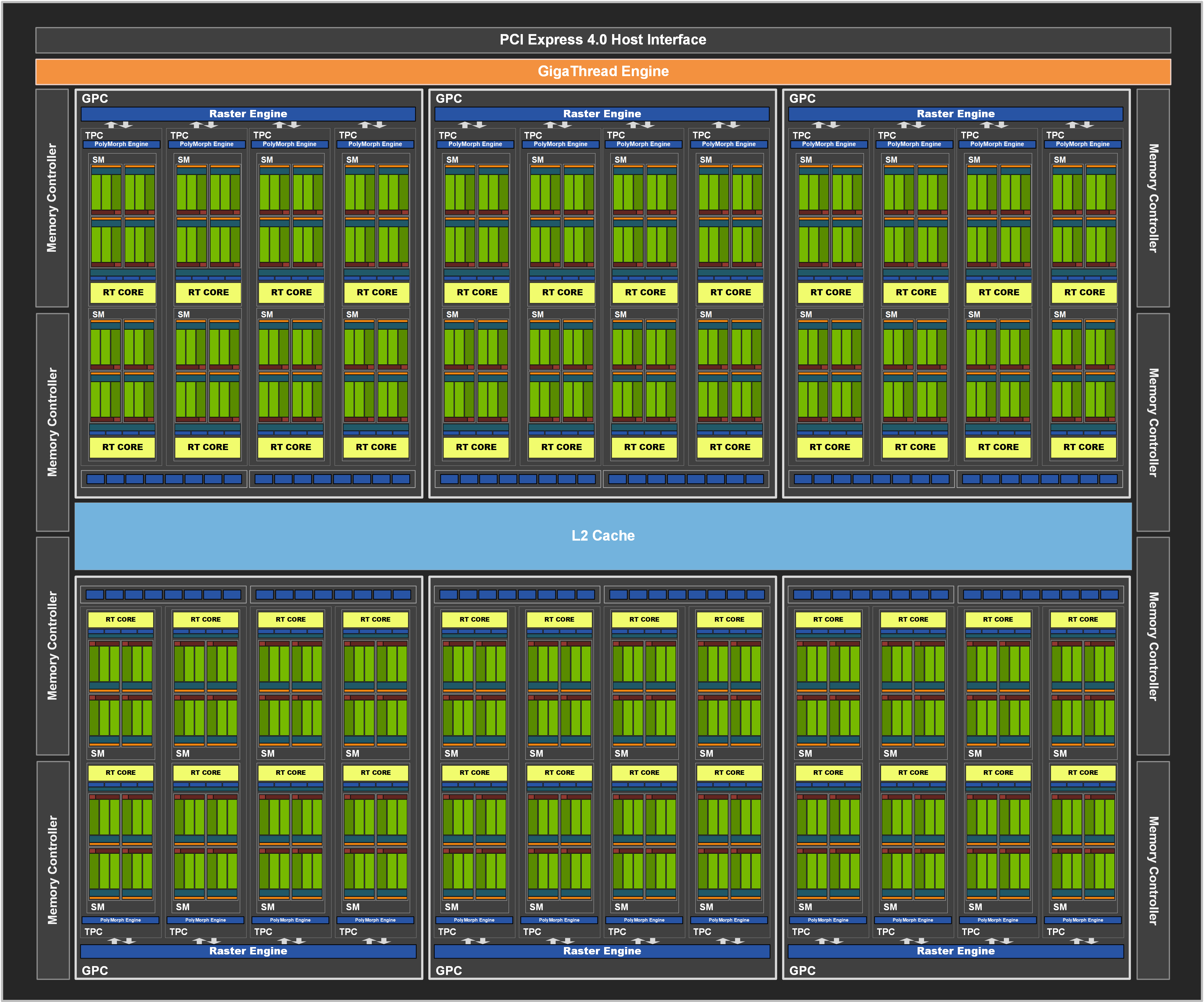
Yeah we were discussing this some pages back that the GPC's in Ampere don't have to be structured the same but every TPC has 2 SM's. GA102 has 6 TPC for 12SM's per GPC, while GA104 has 4TPC's for(8SM's per GPC).We were assuming that the SoC would be using the same hierarchy of GPC/TPC/SMs as seen in Nvidia's other hardware. Namely 1 GPC contains 4 TPCs with 2 SMs each.
But apparently, the GA10F uses a different structure, 1 GPC containing 6 TPCs with 2 SMs each.
GA104
GA102

The $ increase definitely lines up with what we were expecting for Lovelace and the supposed leaked desktop 40 series cards $ numbers also shows Nvidia chasing AMD's infinity cache solution.Some more numbers, apparently. L2 cache = 4 * 1024 * 1024 = 4 MB (same as GA10B). RT core count = 12 (GA10B = 16).
To the obvious follow-up question, no, I still have no context for these numbers.
- Pronouns
- He/Him
Probably not thicker, no. The die needs more room in the same horizontal plane, it shouldn't require more room in the depth direction unless they're really cranking up the clocks to the extent that additional cooling is needed which seems exceedingly unlikely.What if this new model is chonkier, i.e. like the Steam Deck? Would that make the whole 12SM thing feasable?
A bigger die consumes less power for the Dane performance, at least on most of the power curve. A big die is one way they can keep this thing cool and give it a long battery life.
If theyre going with 12 sm, it likely means very low clock speeds. Low clock speeds means less heat.So does that mean the fan noise will potentially be the same or quieter than the OG Switch? Hopefully nothing like Steam Deck.
cw_sasuke
Octorok
I think they are gonna try to establish the 400 price point for the best Hybrid system they offer at any given time.This system needs to be $399 for me
300 for the last gen hybrid offering, 200 including a game for the portable only last gen offering.
thegodsend
Tektite
- Pronouns
- he/him
Are there any caveats performance-wise in using a bigger SoC with 12SM and lower clockspeeds compared to 8SM and higher clockspeeds?
Or is it a clever approach to avoid heat as long as the SoC fits within the overall Switch shell?
Or is it a clever approach to avoid heat as long as the SoC fits within the overall Switch shell?
Ghostsonplanets
Ghost in the Sales
- Pronouns
- He/Him
GA10F is Drake right? So that means that unlike Orin, which is 2 GPCs with 4 TPC each, Drake is just one GPC with 6 TPC, like GA102. That's interesting and points out to T239(Nintendo chip) being a further custom chip that what we thought before. And yeah, if it's 1 GPC with 6 TPC, it means 12 SMs or 1536 CUDA Cores.Some more numbers in case everyone wasn't confused enough. GA10F has 1 GPC with 6 TPC. GA10B has 2 GPC with 4 TPC per (8 total).
I've also been shown some numbers for GA10B and GA10F floating-point efficiency, but I'm scared to post them.
You can think of warp as a thread. In GPUs, they're usually done in 32 or 64 warps(i.e A warp is issued to 32/64 CUDA cores in parallel). Ampere, according to this:What does warp count mean?
So that means the number of warps that can be executed in parallel is slightly reduced on T239. Maybe because of occupancy issues? I don't know.The maximum number of concurrent warps per SM remains the same as in Volta (i.e., 64)
12 SMs sounds too big chip for Switch like device, if we talk about 8nm.
While is easy to think this, 12 SMs aren't that big actually. Take GA107(Die used for RTX 3050, 2050 and MX570), which is manufactured on Samsung 8N. GA107 is a 20 SM die. Despite this, the size on Samsung 8N is 19Xmm²(X means a number between 0 and 9). A 12 SM GPU die would be much smaller than that.What if this new model is chonkier, i.e. like the Steam Deck? Would that make the whole 12SM thing feasable?
- Pronouns
- He/Him
$$$$Are there any caveats performance-wise in using a bigger SoC with 12SM and lower clockspeeds compared to 8SM and higher clockspeeds?
Or is it a clever approach to avoid heat as long as the SoC fits within the overall Switch shell?
Bigger chips cost more money, you need more wafers to get the same amount of chips.
And also space. It needs to fit in the same or similar form factor to the OG Switch in all likelihood, and there's not that much extra room in there. They'll need to redesign something a bit to fit a ~50% bigger die (or whatever the size winds up being). EDIT: Oh you acknowledged space. Yeah.
ArchedThunder
Uncle Beerus
- Pronouns
- He/Him
I hope the dock has active cooling so the docked clock speeds can be turned up to a decent degree.
Also, another benefit of going with more SMs is more tensor cores, right?
Also, another benefit of going with more SMs is more tensor cores, right?
- Pronouns
- He/Him
And more RT cores, yeah.I hope the dock has active cooling so the docked clock speeds can be turned up to a decent degree.
Also, another benefit of going with more SMs is more tensor cores, right?
BlueManifest
Bob-omb
I know TFs don’t matter and such but how many will this have if they downclock for heat
- Pronouns
- He/Him
At Switch's current portable clocks, between 0.9TF and 1.4TF. I can't remember the docked clocks but Zombie indicated something like 3-3.5TF.I know TFs don’t matter and such but how many will this have if they downclock for heat
BlueManifest
Bob-omb
Where is zombie during all these leaksAt Switch's current portable clocks, between 0.9TF and 1.4TF. I can't remember the docked clocks but Zombie indicated something like 3-3.5TF.
- Pronouns
- He/Him
In the discord.Where is zombie during all these leaks
OP
OP
Generally speaking, bigger chips have a lower yield rate than smaller chips.Are there any caveats performance-wise in using a bigger SoC with 12SM and lower clockspeeds compared to 8SM and higher clockspeeds?
Or is it a clever approach to avoid heat as long as the SoC fits within the overall Switch shell?
Also generally speaking lower clocked chips gave better yields than higher.Generally speaking, bigger chips have a lower yield rate than smaller chips.
So there is a sweetspot somewhere.
IamPeacock
Piranha Plant
- Pronouns
- Him / His
I wonder if Nvidia is hoping that with providing the next Nintendo system with DLSS capabilities, it will encourage more third publishers to add DLSS to their games.
This could mean a bigger incentive for publishers to add it, because they can now benefit from the effort on multiple platforms (PC and Switch).
This could mean a bigger incentive for publishers to add it, because they can now benefit from the effort on multiple platforms (PC and Switch).
Thraktor
"[✄]. [✄]. [✄]. [✄]." -Microsoft
- Pronouns
- He/Him
I'm going to again preface this by saying I have a shallow understanding of the things I'm seeing at this point. But this certainly seems relevant to the thread.
NVN v1 source has a constants file with the following:
C:// Number of warps per SM on TX1 hardware #define __NVN_NUM_WARPS_PER_SM_TX1 128 // Number of SMs on TX1 hardware #define __NVN_NUM_SMS_TX1 2
NVN v2 source replaces them with this:
C:// Number of warps per SM on ga10f #define __NVN_NUM_WARPS_PER_SM_GA10F 48 // Number of SMs on on ga10f #define __NVN_NUM_SMS_GA10F 12
I told you all it wouldn't have 8 SMs!

Seriously, though, that's nuts. Like "I know this is coming from a hack from Nvidia and Nvidia have actually confirmed the hack happened but I still kind of think it's fake" nuts. On 8nm, even ignoring portable mode for a moment, I can't even see them running all 12 SMs in docked mode in the same form factor as the base Switch, at least not without a very loud fan. Off the top of my head, I can think of the following possibilities:
- The T239-based Switch "Pro" was a TV-only console all along. This makes less business sense to me (a hybrid device would sell more, justifying the development costs), but it would make a larger, more power-hungry chip much more reasonable.
- This isn't Samsung 8nm (and it seems kopite isn't sure on this any more). My guess would be a Samsung 5nm process, but it could be anything. Even on a TSMC 5nm process (which I still think is very unlikely), I'd be surprised to see them running all 12 SMs at any clock in portable mode.
- They're disabling some of the SMs in portable mode, cutting it down to 6 SMs, or even just 4, to save power.
Yeah, the thing is, if you do the math with those numbers, the chip would only have 576 CUDA cores, which is only a bit more than double the current Switch's 256.
Unless the warp count doesn't directly correspond to CUDA cores. I'll admit this is pretty out of my depth on GPU architecture.
Warp counts aren't related to CUDA cores, it's more about the amount of register memory and the capability of the thread scheduler and stuff like that. The actual amount of warps you can run concurrently on an SM isn't always exactly that max, either, depending on how you're using them. It does indicate that there are more low-level differences between desktop Ampere and T239 than we're aware of, but my guess is that it's probably shared with Orin, and may be one of a number of low-level optimisations around power consumption.
I'm very curious to hear what @Thraktor thinks about this seemingly confirming 12 SMs. My views on the hardware have typically aligned with his and this is throwing me for a loop.
Makes sense, thank you. I didn't consider that there'd be two sides to it.
Thraktor is very confused!
I don't know what "FLCG" is exactly, but it is related to clock gating, and a comment states that GA10F is the only Ampere chip which supports FLCG. Could be an indication of downclocking for portable mode? Just a guess though.
Clock gating means being able to stop delivering a clock signal to certain functional units to save power. Specifically in this case, it means being able to disable some SMs while keeping others running. So it would very much look like point 3 above is true, and they're looking at disabling SMs in portable mode.
OP
OP
I think TSMC's N6 process node being used for the fabrication of Drake is probably the best case scenario, considering that Nvidia probably paid a premium to secure enough capacity for TSMC's N5 process node for datacentre chips (e.g. Hopper, Grace), and at the very least, high-end Lovelace GPUs.
- This isn't Samsung 8nm (and it seems kopite isn't sure on this any more). My guess would be a Samsung 5nm process, but it could be anything. Even on a TSMC 5nm process (which I still think is very unlikely), I'd be surprised to see them running all 12 SMs at any clock in portable mode.
- Pronouns
- He/Him
Thank you for that dose of reality, that makes much more sense to me than all 12 being active in portable mode.I told you all it wouldn't have 8 SMs!
Seriously, though, that's nuts. Like "I know this is coming from a hack from Nvidia and Nvidia have actually confirmed the hack happened but I still kind of think it's fake" nuts. On 8nm, even ignoring portable mode for a moment, I can't even see them running all 12 SMs in docked mode in the same form factor as the base Switch, at least not without a very loud fan. Off the top of my head, I can think of the following possibilities:
My guess is a combination of 2 and 3. Samsung 5nm process of some kind and running only 6 SMs while in portable mode. With portable/docked clocks of 400/800MHz (being a bit conservative here), that would put us at about 600 Gflops handheld and 2.4 Tflops docked. This actually makes some sense when you consider the much bigger resolution difference between handheld and docked once 4K comes into play. The original Switch had a roughly 2x difference in resolution between 720p and 1080p, and roughly a 2x difference in performance. Here we have a 4x difference in performance, and possibly a 4x difference in resolution from 1080p handheld to 4K docked.
- The T239-based Switch "Pro" was a TV-only console all along. This makes less business sense to me (a hybrid device would sell more, justifying the development costs), but it would make a larger, more power-hungry chip much more reasonable.
- This isn't Samsung 8nm (and it seems kopite isn't sure on this any more). My guess would be a Samsung 5nm process, but it could be anything. Even on a TSMC 5nm process (which I still think is very unlikely), I'd be surprised to see them running all 12 SMs at any clock in portable mode.
- They're disabling some of the SMs in portable mode, cutting it down to 6 SMs, or even just 4, to save power.
Warp counts aren't related to CUDA cores, it's more about the amount of register memory and the capability of the thread scheduler and stuff like that. The actual amount of warps you can run concurrently on an SM isn't always exactly that max, either, depending on how you're using them. It does indicate that there are more low-level differences between desktop Ampere and T239 than we're aware of, but my guess is that it's probably shared with Orin, and may be one of a number of low-level optimisations around power consumption.
Thraktor is very confused!
Clock gating means being able to stop delivering a clock signal to certain functional units to save power. Specifically in this case, it means being able to disable some SMs while keeping others running. So it would very much look like point 3 above is true, and they're looking at disabling SMs in portable mode.
Isn’t it a possibility that all sms are active in portable, they’re just clocked absurdly low?I told you all it wouldn't have 8 SMs!
Seriously, though, that's nuts. Like "I know this is coming from a hack from Nvidia and Nvidia have actually confirmed the hack happened but I still kind of think it's fake" nuts. On 8nm, even ignoring portable mode for a moment, I can't even see them running all 12 SMs in docked mode in the same form factor as the base Switch, at least not without a very loud fan. Off the top of my head, I can think of the following possibilities:
My guess is a combination of 2 and 3. Samsung 5nm process of some kind and running only 6 SMs while in portable mode. With portable/docked clocks of 400/800MHz (being a bit conservative here), that would put us at about 600 Gflops handheld and 2.4 Tflops docked. This actually makes some sense when you consider the much bigger resolution difference between handheld and docked once 4K comes into play. The original Switch had a roughly 2x difference in resolution between 720p and 1080p, and roughly a 2x difference in performance. Here we have a 4x difference in performance, and possibly a 4x difference in resolution from 1080p handheld to 4K docked.
- The T239-based Switch "Pro" was a TV-only console all along. This makes less business sense to me (a hybrid device would sell more, justifying the development costs), but it would make a larger, more power-hungry chip much more reasonable.
- This isn't Samsung 8nm (and it seems kopite isn't sure on this any more). My guess would be a Samsung 5nm process, but it could be anything. Even on a TSMC 5nm process (which I still think is very unlikely), I'd be surprised to see them running all 12 SMs at any clock in portable mode.
- They're disabling some of the SMs in portable mode, cutting it down to 6 SMs, or even just 4, to save power.
Warp counts aren't related to CUDA cores, it's more about the amount of register memory and the capability of the thread scheduler and stuff like that. The actual amount of warps you can run concurrently on an SM isn't always exactly that max, either, depending on how you're using them. It does indicate that there are more low-level differences between desktop Ampere and T239 than we're aware of, but my guess is that it's probably shared with Orin, and may be one of a number of low-level optimisations around power consumption.
Thraktor is very confused!
Clock gating means being able to stop delivering a clock signal to certain functional units to save power. Specifically in this case, it means being able to disable some SMs while keeping others running. So it would very much look like point 3 above is true, and they're looking at disabling SMs in portable mode.
BlueManifest
Bob-omb
I think it needs 1 TF minimum in portable mode, 600 gflops isn’t a huge leap from the current switchI told you all it wouldn't have 8 SMs!
Seriously, though, that's nuts. Like "I know this is coming from a hack from Nvidia and Nvidia have actually confirmed the hack happened but I still kind of think it's fake" nuts. On 8nm, even ignoring portable mode for a moment, I can't even see them running all 12 SMs in docked mode in the same form factor as the base Switch, at least not without a very loud fan. Off the top of my head, I can think of the following possibilities:
My guess is a combination of 2 and 3. Samsung 5nm process of some kind and running only 6 SMs while in portable mode. With portable/docked clocks of 400/800MHz (being a bit conservative here), that would put us at about 600 Gflops handheld and 2.4 Tflops docked. This actually makes some sense when you consider the much bigger resolution difference between handheld and docked once 4K comes into play. The original Switch had a roughly 2x difference in resolution between 720p and 1080p, and roughly a 2x difference in performance. Here we have a 4x difference in performance, and possibly a 4x difference in resolution from 1080p handheld to 4K docked.
- The T239-based Switch "Pro" was a TV-only console all along. This makes less business sense to me (a hybrid device would sell more, justifying the development costs), but it would make a larger, more power-hungry chip much more reasonable.
- This isn't Samsung 8nm (and it seems kopite isn't sure on this any more). My guess would be a Samsung 5nm process, but it could be anything. Even on a TSMC 5nm process (which I still think is very unlikely), I'd be surprised to see them running all 12 SMs at any clock in portable mode.
- They're disabling some of the SMs in portable mode, cutting it down to 6 SMs, or even just 4, to save power.
Warp counts aren't related to CUDA cores, it's more about the amount of register memory and the capability of the thread scheduler and stuff like that. The actual amount of warps you can run concurrently on an SM isn't always exactly that max, either, depending on how you're using them. It does indicate that there are more low-level differences between desktop Ampere and T239 than we're aware of, but my guess is that it's probably shared with Orin, and may be one of a number of low-level optimisations around power consumption.
Thraktor is very confused!
Clock gating means being able to stop delivering a clock signal to certain functional units to save power. Specifically in this case, it means being able to disable some SMs while keeping others running. So it would very much look like point 3 above is true, and they're looking at disabling SMs in portable mode.
D
Deleted member 645
Guest
Well at least concrete things to discuss.
600 tflops ampere with a much less bottlenecked design, dlss and still targeting 720p, is a huge leap.I think it needs 1 TF minimum in portable mode, 600 gflops isn’t a huge leap from the current switch
Kenka
Like Like
- Pronouns
- He/Him
While it isn't the biggest leap possible, I commend Thraktor to come up with a realisitc scenario in the face of the madness that has us (me included) gripped.I think it needs 1 TF minimum in portable mode, 600 gflops isn’t a huge leap from the current switch
This.600 tflops ampere with a much less bottlenecked design, dlss and still targeting 720p, is a huge leap.
Last edited:
- Pronouns
- He/Him
600 Ampere GFlops is not the same as 600 Maxwell GFlops. It would be a pretty nice boost not even considering CPU/RAM gains and DLSS.I think it needs 1 TF minimum in portable mode, 600 gflops isn’t a huge leap from the current switch
- Pronouns
- He/Him
I’ll go in order from lowest order to highest orderCould anyone explain what GPCs, TPCs, SMs and CUDA cores are?
How relevant are each of these items to determine the power of a chip?
A CUDA Core is an individual GPU core and CUDA stands for Compute Unified Device Architecture, they are a special programming language for which a developer codes their software to. These are like the Cells.
An SM, or Streaming Multiprocessor is the grouping of many individual shading units/cores. They contain CUDA Cores and the SM functions like cell tissue.
The TPC is an organizational format we find on NVIDIA GPUs. A TPC, or Texture Processor Cluster, is a group made up of several SMs (that can vary depending on the architecture), a texture unit and some logic control. It exists in all of NV GPUs since Fermi architecture I think. Think of this like the Organ of the GPU in a way.
The Graphics Processing Cluster (GPC) is a dedicated hardware block for computing, rasterization, shading, and texturing, etc., most of the GPU's core graphical functions are performed inside the GPC, a GPU can have multiple GPCs. Think of this like the organ system of a GPU.
And think of a GPU as an Organism, a reminder of biology but the order of living organisms is Cell>Tissue>Organ>OrganSystem>Organism.
GPUs function in a similar way.
Last edited:
Kenka
Like Like
- Pronouns
- He/Him
Could a fourth possibility be that T239 is a chip for the dock?Seriously, though, that's nuts. Like "I know this is coming from a hack from Nvidia and Nvidia have actually confirmed the hack happened but I still kind of think it's fake" nuts. On 8nm, even ignoring portable mode for a moment, I can't even see them running all 12 SMs in docked mode in the same form factor as the base Switch, at least not without a very loud fan. Off the top of my head, I can think of the following possibilities:
- The T239-based Switch "Pro" was a TV-only console all along. This makes less business sense to me (a hybrid device would sell more, justifying the development costs), but it would make a larger, more power-hungry chip much more reasonable.
- This isn't Samsung 8nm (and it seems kopite isn't sure on this any more). My guess would be a Samsung 5nm process, but it could be anything. Even on a TSMC 5nm process (which I still think is very unlikely), I'd be surprised to see them running all 12 SMs at any clock in portable mode.
- They're disabling some of the SMs in portable mode, cutting it down to 6 SMs, or even just 4, to save power.
What an amazing description. I love you!I’ll go in order from lowest order to highest order
A CUDA Core is an individual GPU core and CUDA stands for Compute Unified Device Architecture, they are a special programming language for which a developer codes their software to. These are like the Cells.
An SM, or Streaming Multiprocessor is the grouping of many individual shading units/cores. They contain CUDA Cores and the SM functions like cell tissue.
The TPC is an organizational format we find on NVIDIA GPUs. A TPC, or Texture Processor Cluster, is a group made up of several SMs (that can vary depending on the architecture), a texture unit and some logic control. It exists in all of NV GPUs since Fermi architecture I think. Think of this like the Organ of the GPU in a way.
The Graphics Processing Cluster (GPC) is a dedicated hardware block for computing, rasterization, shading, and texturing; most of the GPU's core graphics functions are performed inside the GPC. Think of this like the organ system of a GPU.
And think of a GPU as an Organism, a reminder of biology but the order of living organisms is Cell>Tissue>Organ>OrganSystem>Organism.
GPUs function in a similar way.
@Dakhil why not add this to the OP?I’ll go in order from lowest order to highest order
A CUDA Core is an individual GPU core and CUDA stands for Compute Unified Device Architecture, they are a special programming language for which a developer codes their software to. These are like the Cells.
An SM, or Streaming Multiprocessor is the grouping of many individual shading units/cores. They contain CUDA Cores and the SM functions like cell tissue.
The TPC is an organizational format we find on NVIDIA GPUs. A TPC, or Texture Processor Cluster, is a group made up of several SMs (that can vary depending on the architecture), a texture unit and some logic control. It exists in all of NV GPUs since Fermi architecture I think. Think of this like the Organ of the GPU in a way.
The Graphics Processing Cluster (GPC) is a dedicated hardware block for computing, rasterization, shading, and texturing; most of the GPU's core graphics functions are performed inside the GPC. Think of this like the organ system of a GPU.
And think of a GPU as an Organism, a reminder of biology but the order of living organisms is Cell>Tissue>Organ>OrganSystem>Organism.
GPUs function in a similar way.
- Pronouns
- He/Him
That's very unlikely. That would be massive overkill for an eGPU, and nothing else conceptually could work.Could a fourth possibility be that T239 is a chip for the dock?
- Pronouns
- He/Him
My sourcing was of course google for most of it, but I formatted it in a way that makes it more clear on the hierarchy of it all.
ArchedThunder
Uncle Beerus
- Pronouns
- He/Him
Wouldn’t turning SMs on and off be a lot harder than just adjusting clocks when switching between handheld and docked?
- Pronouns
- He/Him
Nah, it should be essentially just as simple. You're doing the same thing, changing the amount of voltage you're applying to certain areas of the GPU. It should be indistinguishable from changing clocks as far as game developers and end users are concerned.Wouldn’t turning SMs on and off be a lot harder than just adjusting clocks when switching between handheld and docked?
Z0m3le
Bob-omb
We should look at the GA107S to get some grounds for this discussion. Here we see a 16SM GPU clocked at 1.2GHz with 4GB of GDDR6 memory and a TDP of 25 watts. The memory takes up ~8 watts here, so the TDP of the GPU is about ~17 watts, so lets say it's 13 watts on the same 8nm node for the same 1.2GHz clock on Drake. However we can reduce the clock to 1GHz and see a huge reduction in power consumption, lets error on the side of caution and say 30% for a 17% clock reduction, now we are looking at 10 watts for Drake's GPU when docked.I told you all it wouldn't have 8 SMs!
Seriously, though, that's nuts. Like "I know this is coming from a hack from Nvidia and Nvidia have actually confirmed the hack happened but I still kind of think it's fake" nuts. On 8nm, even ignoring portable mode for a moment, I can't even see them running all 12 SMs in docked mode in the same form factor as the base Switch, at least not without a very loud fan. Off the top of my head, I can think of the following possibilities:
My guess is a combination of 2 and 3. Samsung 5nm process of some kind and running only 6 SMs while in portable mode. With portable/docked clocks of 400/800MHz (being a bit conservative here), that would put us at about 600 Gflops handheld and 2.4 Tflops docked. This actually makes some sense when you consider the much bigger resolution difference between handheld and docked once 4K comes into play. The original Switch had a roughly 2x difference in resolution between 720p and 1080p, and roughly a 2x difference in performance. Here we have a 4x difference in performance, and possibly a 4x difference in resolution from 1080p handheld to 4K docked.
- The T239-based Switch "Pro" was a TV-only console all along. This makes less business sense to me (a hybrid device would sell more, justifying the development costs), but it would make a larger, more power-hungry chip much more reasonable.
- This isn't Samsung 8nm (and it seems kopite isn't sure on this any more). My guess would be a Samsung 5nm process, but it could be anything. Even on a TSMC 5nm process (which I still think is very unlikely), I'd be surprised to see them running all 12 SMs at any clock in portable mode.
- They're disabling some of the SMs in portable mode, cutting it down to 6 SMs, or even just 4, to save power.
Warp counts aren't related to CUDA cores, it's more about the amount of register memory and the capability of the thread scheduler and stuff like that. The actual amount of warps you can run concurrently on an SM isn't always exactly that max, either, depending on how you're using them. It does indicate that there are more low-level differences between desktop Ampere and T239 than we're aware of, but my guess is that it's probably shared with Orin, and may be one of a number of low-level optimisations around power consumption.
Thraktor is very confused!
Clock gating means being able to stop delivering a clock signal to certain functional units to save power. Specifically in this case, it means being able to disable some SMs while keeping others running. So it would very much look like point 3 above is true, and they're looking at disabling SMs in portable mode.
I think docked, Drake could be anywhere from 768MHz to 1GHz, offering 2.36TFLOPs to 3TFLOPs when docked. When portable, a 400MHz clock should drastically reduce the GPU power consumption further, lets just go with under 5 watts for the GPU. The big question is will Nintendo allow Drake to use more energy than the original Switch? I think it is very possible, battery technology has gotten much better, so there should be room to pull 10 watts (original Switch was 9 watts with full brightness on a bad screen).
It's also worth noting that it could be 8ULA and not Ampere's current process node, it could even be Samsung's 7nm process node, as we have seen Nvidia shrink an 8nm SoC to 7nm recently. Since the leaker is unsure about the process node, and he is the only source for 8nm, and that GA10F is very likely seen a few changes over the past 3 years... We can no longer assume it is still 8nm. I also think it is a bit reckless to solidify the idea that they would disable Two 3rds of the GPU for portable mode, if that were the case, they would just shrink the GPU and run it at a higher clock instead, as it would save money.
Crusters
Koopa
- Pronouns
- He/him
Isn’t it a possibility that all sms are active in portable, they’re just clocked absurdly low?
Sure. I mean we have nothing but possibilities everywhere you look right now.
But the fact T239 is specifically the only ampere product in this bunch that supports clock hating is kinda hard to get around.
- Pronouns
- He/Him
So from what I remember about this SM discussion in the past, there's a certain point on the power curve where clocking a high SM die too low becomes very inefficient. You wind up using more power to get worse performance at a low enough clock speed, compared to fewer SMs.Isn’t it a possibility that all sms are active in portable, they’re just clocked absurdly low?
So without knowing exactly how the power requirements for this device scale it's hard to know how low they can possibly clock it before it becomes detrimental.
Clock hating?Sure. I mean we have nothing but possibilities everywhere you look right now.
But the fact T239 is specifically the only ampere product in this bunch that supports clock hating is kinda hard to get around.
Crusters
Koopa
- Pronouns
- He/him
That's a typo. Or I've spent too much time in xb3 threads lol.Clock hating?
Clock gating
NineTailSage
Bob-omb
That's the thing it isn't 100% clear anymore if it's on 8nm, we haven't even received confirmation if Orin is manufactured on Samsung's 8nm either...12 SMs sounds too big chip for Switch like device, if we talk about 8nm.
I also hope they have some kind of forced induction cooling design for the dock.I hope the dock has active cooling so the docked clock speeds can be turned up to a decent degree.
Also, another benefit of going with more SMs is more tensor cores, right?
I told you all it wouldn't have 8 SMs!
Seriously, though, that's nuts. Like "I know this is coming from a hack from Nvidia and Nvidia have actually confirmed the hack happened but I still kind of think it's fake" nuts. On 8nm, even ignoring portable mode for a moment, I can't even see them running all 12 SMs in docked mode in the same form factor as the base Switch, at least not without a very loud fan. Off the top of my head, I can think of the following possibilities:
My guess is a combination of 2 and 3. Samsung 5nm process of some kind and running only 6 SMs while in portable mode. With portable/docked clocks of 400/800MHz (being a bit conservative here), that would put us at about 600 Gflops handheld and 2.4 Tflops docked. This actually makes some sense when you consider the much bigger resolution difference between handheld and docked once 4K comes into play. The original Switch had a roughly 2x difference in resolution between 720p and 1080p, and roughly a 2x difference in performance. Here we have a 4x difference in performance, and possibly a 4x difference in resolution from 1080p handheld to 4K docked.
- The T239-based Switch "Pro" was a TV-only console all along. This makes less business sense to me (a hybrid device would sell more, justifying the development costs), but it would make a larger, more power-hungry chip much more reasonable.
- This isn't Samsung 8nm (and it seems kopite isn't sure on this any more). My guess would be a Samsung 5nm process, but it could be anything. Even on a TSMC 5nm process (which I still think is very unlikely), I'd be surprised to see them running all 12 SMs at any clock in portable mode.
- They're disabling some of the SMs in portable mode, cutting it down to 6 SMs, or even just 4, to save power.
Warp counts aren't related to CUDA cores, it's more about the amount of register memory and the capability of the thread scheduler and stuff like that. The actual amount of warps you can run concurrently on an SM isn't always exactly that max, either, depending on how you're using them. It does indicate that there are more low-level differences between desktop Ampere and T239 than we're aware of, but my guess is that it's probably shared with Orin, and may be one of a number of low-level optimisations around power consumption.
Thraktor is very confused!
Clock gating means being able to stop delivering a clock signal to certain functional units to save power. Specifically in this case, it means being able to disable some SMs while keeping others running. So it would very much look like point 3 above is true, and they're looking at disabling SMs in portable mode.
I wonder about how much business Nvidia will even be doing with Samsung this next go-round?
That news headline a day or so ago sounds like Samsung wants to aggressively go after TSMC's customers to secure manufacturing capacity from the likes of Nvidia and AMD.
I do wonder how fluid something like switching on and off SM's will work on the fly for a device like the Switch?
I also definitely feel like this is Nintendo investing into a SoC that they can just die shrink further in the future and get more performance out of.
This Drake design might be the foundation for the next-gen Switch's up to 10yrs...
Was that in the leak that t239 supports clock gating?That's a typo. Or I've spent too much time in xb3 threads lol.
Clock gating
NineTailSage
Bob-omb
This would definitely be a better option for pixel fill rate if say the GPU clocks stay at say 800Mhz across the board but SMs change from 12 docked to 6 in handheld mode.Nah, it should be essentially just as simple. You're doing the same thing, changing the amount of voltage you're applying to certain areas of the GPU. It should be indistinguishable from changing clocks as far as game developers and end users are concerned.
Vanillalite
Bob-omb
It’s a basic unit of execution so a group of threads. Pretty sure it’s an nvidia specific term. AMD’s name is like wavefront or waveform. I’d have to look it up to remember.What does warp count mean?
(I also haven’t done any GPU deep divides or coding since college as I don’t need to do or know any of this for my non gaming dev work lol).
D
Deleted member 645
Guest
Question, when did it become common talk that the next switch would be using dlss?
- Pronouns
- He/Him
Mid-late 2020 IIRC.Question, when did it become common talk that the next switch would be using dlss?
Vanillalite
Bob-omb
It is a pretty nice boost, and the new flops are better as per usual.600 Ampere GFlops is not the same as 600 Maxwell GFlops. It would be a pretty nice boost not even considering CPU/RAM gains and DLSS.
I still think it’ll be an issue even at 720p for complex open world type games that just need the raw compute power for some of the more modern complex world design.
Simba1
Bob-omb
That's the thing it isn't 100% clear anymore if it's on 8nm, we haven't even received confirmation if Orin is manufactured on Samsung's 8nm either...
Funny thing, around month ago when I wrote that there is chance that plans changed and that new Switch hardware is not on 8nm like 1st rumors suggested and that will not be released this year, few people attack me here and one even answer me that there is also "chance that we will be hit by meteorite".

Last edited:
Threadmarks
View all 18 threadmarks
Reader mode
Reader mode
Recent threadmarks
Poll #3: When do you think is the launch window for Nintendo's new hardware? Announcement regarding links to news and rumours from 2022 and 2021 Rough summary of the 2 August 2023 episode of Nate the Hate Rough summary of the 11 September 2023 episode of Nate the Hate Anatole's deep dive into a convolutional autoencoder Differences between T234 and T239 Rough summary of the 19 October 2023 episode of Nate the Hate necrolipe's Twitter (X) post on why a 2025 launch doesn't automatically make T239 outdated based on one of the leaked slides from Microsoft
Staff Communication
View all 13 threadmarks
Reader mode
Reader mode
Recent threadmarks
Staff Communication 05/26/23 Staff Post about Citing Leaks and Rumors Staff Post about reading Hidden Content Staff Post- Please read Keeping on topic New Switch 2 ST Made - Nontechnical Talk Has A New Home Staff Post Regarding Dubious Insiders And Better Sourcing Reminder about hide tags NewPlease read this staff post before posting.
Furthermore, according to this follow-up post, all off-topic chat will be moderated.
Furthermore, according to this follow-up post, all off-topic chat will be moderated.
Last edited: