
Sol
Bob-omb
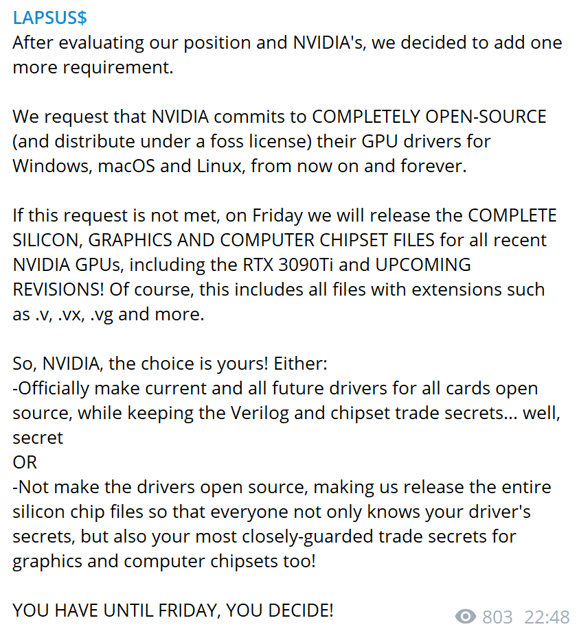
These people will be in jail by Friday.
I may be asking too much but..........Where are you seeing this? I haven't seen any new leaked data so far.NVN2 has added lots of documentation relating to ray tracing, so that's confirmed for the next model, as well as relating to DLSS. You know, just in case anybody was still wondering whether that's confirmed.
Well they say 250GB of Hardware info is in there so Drake's exact specs (As of when the data was pulled) likely are in there too.Saying that, I wonder how much more information is going to be unveiled about Drake on Friday, assuming Nvidia's not going to capitulate to the hacker's demands.
Eh I don't really have faith of that. It's really hard to catch cyber criminals like these. The Capcom ransomware guys never got caught.These people will be in jail by Friday.
I think that depends on when Nintendo and Nvidia decide to change the process node being used for the fabrication of Drake since that's not a process that's done in a matter of months, but in a matter of years (a minimum of half a year or 6 months). (One example is that GH100 was mentioned to be fabricated using TSMC's N5 process node almost 2 years ago.)I've been wondering if Nintendo has been seeing the silicon shortage as a reason to delay Switch 2 and maybe that gave them and Nvidia time to migrate Dane to a new process node, and with that may have prompted a codename change. Possibly taking the process node change in balance to increase the number of cores and/or clockspeed for the CPU and/or GPU.
On the same note, with Dane all but done, that could still make it into a product like the Shield.
The T239 part hasn't changed, and that's the chip's official designation. It's unlikely to have changed, it was just probably always Drake and Kopite got that wrong for whatever reason.I've been wondering if Nintendo has been seeing the silicon shortage as a reason to delay Switch 2 and maybe that gave them and Nvidia time to migrate Dane to a new process node, and with that may have prompted a codename change. Possibly taking the process node change in balance to increase the number of cores and/or clockspeed for the CPU and/or GPU.
On the same note, with Dane all but done, that could still make it into a product like the Shield.
These are all things people are finding in the leak. There's 75 GB of data, so the handful of screencaps on Twitter is certainly not all of it.I may be asking too much but..........Where are you seeing this? I haven't seen any new leaked data so far.
One interesting thing I saw was that, out of several lists of forbidden words (that are meant to be scanned for before something is released to the public) which had "drake" on them, one of them also had "dane." So that name was considered sensitive for some reason at some point.The T239 part hasn't changed, and that's the chip's official designation. It's unlikely to have changed, it was just probably always Drake and Kopite got that wrong for whatever reason.
Well now I'm confused all over again.One interesting thing I saw was that, out of several lists of forbidden words (that are meant to be scanned for before something is released to the public) which had "drake" on them, one of them also had "dane." So that name was considered sensitive for some reason at some point.
it means that either the codename changes, or the chip was branched into a new oneWell now I'm confused all over again.
Exactly. Chip shortage was pretty evident in mid-2020. Let's say that they're level headed and by late 2020 made a decision:I think that depends on when Nintendo and Nvidia decide to change process node since that's not a process that's done in a matter of months, but in a matter of years. (One example is that GH100 was mentioned to be fabricated using TSMC's N5 process node almost 2 years ago.)
The codename for Dane leaked early last year, them going with a new one doesn't surprise me. It could have also been a change to some element of the chip. GA10F is another name for the chip that we know now, considering the alphabet, it is interesting they went all the way to F for the naming of this SoC.Well now I'm confused all over again.
This doesn't add up because Aula was datamined in April 2020, meaning in the works long before the pandemic hit.Exactly. Chip shortage was pretty evident in mid-2020. Let's say that they're level headed and by late 2020 made a decision:
1. Split the current development effort into releasing the OLED that was being saved for Switch 2 as an upgraded Switch 1 in 2021.
1a. Took 239 and started the work to port it to a smaller node and increase the GPU core count by 2.
2. Release the OLED Switch in late 2021.
3. Plan to release Switch 2 late 2022 or 6 year anniversary or Late 2023 depending on a number of factors.
This way they get two things.
1. They get the cost benefits of moving to OLED.
2. If there was some unhappiness about what hardware fit into the power envelope, they get a chance to adjust it.
It may have been that they were worried about an anemic and launch of Switch 2 anyway.
It just seems like a whole jumble of costs and benefits to me, but I feel like it's worth thinking about.
Congrats, @DakhilI won't be able to summarise what NateDrake and MVG said right away since I'm starting my first day of work tomorrow after job searching for more than a year.
Thank you. I definitely got really lucky.Congrats, @Dakhil
Finding a job—especially in this climate—can be tough, but I'm glad you were eventually successful. Good luck to you!
So that means Nintendo could enable HDR support for the OLED model in the future?The NVN2 documentation also says that HDR is supported, both as part of DLSS and as a new feature in the core NVN API.
considering it's not there now, I doubt enabling support is a thing on their mindsSo that means Nintendo could enable HDR support for the OLED model in the future?
I thought this leaked today? I don't remember Drake from 2020. Maybe the catalyst was earlier. Maybe it was going to be Aula and Dane side-by-side, but Dane got delayed. Maybe Aula was originally just a Switch Lite revision 2DS Style.This doesn't add up because Aula was datamined in April 2020, meaning in the works long before the pandemic hit.
I was talking about theoretically speaking rather in actually speaking. But yeah, I personally don't expect Nintendo to enable HDR support for the OLED model anytime soon.considering it's not there now, I doubt enabling support is a thing on their minds
It's not clear to me from what's been shown whether NVN2 is supported on pre-Ampere GPUs, but I'm leaning toward no. The language around GPU/arch support is all related to the Windows implementation (i.e. things to be aware of since your development PC might not behave exactly like the NX hardware you're actually targeting), and I haven't yet seen anywhere that's like "this model of NX can do this, but this other one can't." So that implies the NVN2 documentation is only concerned with one NX model, which would have to be the new one since the old one (as far as we know) can't do DLSS and ray tracing.So that means Nintendo could enable HDR support for the OLED model in the future?
Thanks for the clarification. That does make sense.It's not clear to me from what's been shown whether NVN2 is supported on pre-Ampere GPUs, but I'm leaning toward no. The language around GPU/arch support is all related to the Windows implementation (i.e. things to be aware of since your development PC might not behave exactly like the NX hardware you're actually targeting), and I haven't yet seen anywhere that's like "this model of NX can do this, but this other one can't." So that implies the NVN2 documentation is only concerned with one NX model, which would have to be the new one since the old one (as far as we know) can't do DLSS and ray tracing.
Thank you for that explanation, honestly I agree entirely and I just never knew how to put it in words where it made sense haha. A cross-gen spectrum absolutely makes the most sense for how the Switch and any future iterations would be supported.Don't think about "revision" or "successor" think about "cross-gen support" as a spectrum.
On one end of the spectrum, all games released going forward run on both devices, and when support stops for the Old Switch it stops for the Nu Switch at the same time (close to New 3DS, or DSi level revision).
On the other end of the spectrum, there are a few cross-gen games, but they are different versions that you have to buy seperately, and all first party dev moves to the "new" machine (the WiiU).
There are lots of options in between. Like, for example, lots of cross-gen games for a few years, but eventually all games are exclusive to the Nu Switch which slowly takes over for a "generation" that runs like 12 years - the Game Boy Color model.
Lots of folk saying "Successor" or "revision" is a marketing term, but if the device is backwards compatible, then it's as much about "how does first party support shift" which is a decision that Nintendo can change* after the launch of the device.
*I recognize that it is really hard to turn that ship, just that Nintendo can retool if things go wrong. Just as they kept 3DS on life support until they were sure Switch took off, or GBA until the DS was solid
Even if HDR isn't implemented on the OLED for gaming, is it at all possible if streaming platforms like Netflix or Disney+ get added in the future, HDR could be enabled for OLED consoles via firmware updates given their docks also support HDMI 2.0?So that means Nintendo could enable HDR support for the OLED model in the future?
It's been a while since Nvidia produced an SoC that would be appropriate for a game console, but they have produced a few between TX1 and Orin. It's probably mostly a function of most of Nvidia's non-Nintendo SoC customers having pretty specialized needs.Truly don't know, and honestly something I would wonder too. It seems AMD releases these Zen chipsets every year or every other year. The Nvidia SoC that people reference, I was under the impression come out every 7 or 8 years, do they not?
Hard to say what this means without knowing how Nvidia treats codenames internally.One interesting thing I saw was that, out of several lists of forbidden words (that are meant to be scanned for before something is released to the public) which had "drake" on them, one of them also had "dane." So that name was considered sensitive for some reason at some point.
I'm talking about Aula, not Drake. Aula was datamined in 2020 so the OLED model (which is Aula) was planned far before the pandemic hit. And everything in that original datamined remained accurate when the OLED model launched, so plans for the OLED model did not change at all after the onset of the pandemic and the chip shortage.I thought this leaked today? I don't remember Drake from 2020. Maybe the catalyst was earlier. Maybe it was going to be Aula and Dane side-by-side, but Dane got delayed. Maybe Aula was originally just a Switch Lite revision 2DS Style.
Please remember that I'm not making claims, but instead exploring a line of reasoning. I'm not trying to prognosticate.
Maybe Shulk had a vision!So the theory that the OLED model was some stopgap or branch thrown together due to the pandemic cannot be accurate with what we know.
I wouldn't be surprised if Dane/Drake's launch title is Xenoblade 3.Maybe Shulk had a vision!
Probably a few more important things he could've done with that vision.Maybe Shulk had a vision!
I think theoretically speaking, yes. But whether or not Nintendo would actually enable HDR support for media is another story altogether.Even if HDR isn't implemented on the OLED for gaming, is it at all possible if streaming platforms like Netflix or Disney+ get added in the future, HDR could be enabled for OLED consoles via firmware updates given their docks also support HDMI 2.0?

I think the question marks are just referring to things this leak has not yet confirmed.I don't fault him on the codename mix up at all, but the ? By the process node is the most interesting out of all of this.
Simply because he was pretty assertive that all the Tegra derivatives would be on 8nm as well...
// Number of warps per SM on TX1 hardware
#define __NVN_NUM_WARPS_PER_SM_TX1                  128

// Number of SMs on TX1 hardware
#define __NVN_NUM_SMS_TX1 2// Number of warps per SM on ga10f
#define __NVN_NUM_WARPS_PER_SM_GA10F 48
// Number of SMs on on ga10f
#define __NVN_NUM_SMS_GA10F 12Dangit, so close to the GPU core count!I'm going to again preface this by saying I have a shallow understanding of the things I'm seeing at this point. But this certainly seems relevant to the thread.
NVN v1 source has a constants file with the following:
C:// Number of warps per SM on TX1 hardware #define __NVN_NUM_WARPS_PER_SM_TX1 128 // Number of SMs on TX1 hardware #define __NVN_NUM_SMS_TX1 2
NVN v2 source replaces them with this:
C:// Number of warps per SM on ga10f #define __NVN_NUM_WARPS_PER_SM_GA10F 48 // Number of SMs on on ga10f #define __NVN_NUM_SMS_GA10F 12
12SM would likely surpass the Seires S if fed enough power before DLSS12 SMs would be far, far more than we're expecting, no?
Those are the numbers. I can't speak to any implications.Dangit, so close to the GPU core count!
Btw, link to the files? XD
EDIT: Stupid Mobile, umm..is the latter Core count a typo? The Number of SMs seems to line up right (12SM Drake!?) But the"Wraps" is off
You can not compare FLOPs across uArchs directly.12 SMs is 6 times Switch power right? In RAW performance and same clocks (400GFLOPs vs 2400 GFLOPS) on docked mode.
And in portable is 200 GFLOPS vs 1200 GFLOPS
My expectation is half of that but a little higher clock.
That 48 seems... weird. If that's the number of shaders in the SM as implied, that seems weirdly low.I'm going to again preface this by saying I have a shallow understanding of the things I'm seeing at this point. But this certainly seems relevant to the thread.
NVN v1 source has a constants file with the following:
C:// Number of warps per SM on TX1 hardware #define __NVN_NUM_WARPS_PER_SM_TX1 128 // Number of SMs on TX1 hardware #define __NVN_NUM_SMS_TX1 2
NVN v2 source replaces them with this:
C:// Number of warps per SM on ga10f #define __NVN_NUM_WARPS_PER_SM_GA10F 48 // Number of SMs on on ga10f #define __NVN_NUM_SMS_GA10F 12
Yeah, it sounds like this will be the API that native Dane/Drake games will use.Those are the numbers. I can't speak to any implications.
I have seen enough to say now that there's no chance of NVN2 running on an old Switch, regardless of feature set. Even on Windows the oldest GPUs supported are Turing (with the note already posted earlier that says Ampere is preferred because it's most compatible with the real NX). Anything older is unsupported in the sense of "it bails/crashes/doesn't compile." Not really surprising, but just since it was asked earlier about HDR in NVN.
The caveat here is that SMs have different configurations in different architectures. So 1 Maxwell SM will have a different number of CUDA cores then 1 Ampere SM.So I'm just learning this terminology - SM means streaming multiprocessors, when I look up how many SMs the Tegra X1 has it's 2, which lines up with the code above. So the new chip has... 12? I am assuming there is no difference in SM count between devkit and final hardware, so that seems like quite a lot more GPU power.
Yeah but we already know the amount of CUDA in a Ampere/Orin SM, 128 cores.The caveat here is that SMs have different configurations in different architectures. So 1 Maxwell SM will have a different number of CUDA cores then 1 Ampere SM.
Yeah, the thing is, if you do the math with those numbers, the chip would only have 576 CUDA cores, which is only a bit more than double the current Switch's 256.The caveat here is that SMs have different configurations in different architectures. So 1 Maxwell SM will have a different number of CUDA cores then 1 Ampere SM.
