~
But 4G/5G would be a more out-there addition and I feel Nintendo may be more inclined to
use the space savings that the uMCP would bring to either make Dane/T239 bigger, make the battery bigger, or add a more complex cooling solution.
Samsung's official statement made no mention of an option to add a 5G modem to the LPDDR5 uMCP. I think what XDA Developers is saying is that the amount of space saved by using the LPDDR5 uMCP can be used to add 5G antennae, etc., elsewhere, not on the LPDDR5 uMCP.
And I'm not very sure if adding a 5G modem to the LPDDR5 uMCP would be necessary for smartphones when smartphone SoCs, like the
Snapdragon 888,
Exynos 2100,
Dimensity 1200, etc., have a 5G modem integrated into the SoC.
Speaking of integrating a 5G modem into the SoC, I imagine designing a SoC with a 5G modem integrated into the SoC, or a 4G modem integrated into the SoC, won't be inexpensive. As for adding an external 5G modem, so far,
external 5G modems seem to run very hot. I'm not sure about the viability of adding an external 4G modem.
~
I don't think using a LPDDR5 uMCP is viable from a thermal standpoint for the DLSS model* since the LPDDR5 RAM and the UFS 3.1 internal storage in the LPDDR5 uMCP would need to run sustained at all times, resulting in the LPDDR5 uMCP becoming very hot.
Smartphones on the other hand are different since the LPDDR5 RAM and the UFS 3.1 internal storage in the LPDDR5 uMCP only needs to run in short bursts, which means the LPDDR5 uMCP rarely becomes hot. And that's why Samsung's currently only touting LPDDR5 uMCP for smartphones.
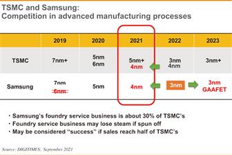
Probably not for Samsung's 5 nm** process nodes. I imagine Nvidia wants to prioritise Samsung's 5 nm** process nodes for higher margin products if Nvidia plans on using Samsung's 5 nm** process nodes for lower end consumer Lovelace GPUs. And
some of Samsung's 5 nm** process nodes are rumoured to have yields below 50%, which seems to be vindicated by
a Xiaomi executive's claim that the reason why the Snapdragon 780G is cancelled is due to lack of capacity. (And there's a
rumour about how Microsoft's and AMD's Arm based SoC was supposed to be fabricated using Samsung's 5 nm** process nodes, but was switched to being fabricated using TSMC's 5 nm** process nodes due to Samsung's 5 nm** process nodes having low yields.)
I don't believe there are any products that are being fabricated using Samsung's 6LPP process node, especially when
Samsung's 6LPP process node is not available to general customers.
Maybe a possibility with Samsung's 7LPP process node? Who knows?
** a marketing nomenclature for all foundry companies


:format(webp):no_upscale()/cdn.vox-cdn.com/uploads/chorus_asset/file/22719673/Image_from_iOS__5_.jpg)