Follow along with the video below to see how to install our site as a web app on your home screen.
Note: This feature currently requires accessing the site using the built-in Safari browser.
Hey everyone, staff have documented a list of banned content and subject matter that we feel are not consistent with site values, and don't make sense to host discussion of on Famiboards. This list (and the relevant reasoning per item) is viewable here.
Furukawa Speaks! We discuss the announcement of the Nintendo Switch Successor and our June Direct Predictions on the new episode of the Famiboards Discussion Club! Check it out here!
Assuming the rumour that Dane's a customised version of Orin is true, physically removing the RT cores from the GPU would be cost prohibitive for Nintendo and Nvidia. Also, NateDrake mentioned that late 2020 devkits have limited RTX support; and I imagine there's no reason to include limited RTX support if there was no plans to use RT cores.
Edit: Woops, I totally misread your comment. Considering Nvidia has made no mention of which generation the RT cores on Orin are part of, there's definitely a possibility.
some old videos (by Nvidia) to set the scene with the idea of DLSS improving denoising
a good overview of denoising
Nvidia already has a machine learned denoiser, Optix, but it doesn't run in real time. they do have a realtime denoiser, which is already used in games
as they mention, it's usable with .5 or 1 ray per pixel. if Nvidia gets their machine learned denoiser to work in real-time, and with .25 rays per pixel, that could be a big increase in performance. question is, is ¼ res enough information? at 4K, that's 540p being upscaled to 2160p. we've seen some games do this and it looked assy (Resident Evil Village). a better denoiser might help that
Assuming the rumour that Dane's a customised version of Orin is true, physically removing the RT cores from the GPU would be cost prohibitive for Nintendo and Nvidia. Also, NateDrake mentioned that late 2020 devkits have limited RTX support; and I imagine there's no reason to include limited RTX support if there was no plans to use RT cores.
Assuming the rumour that Dane's a customised version of Orin is true, physically removing the RT cores from the GPU would be cost prohibitive for Nintendo and Nvidia. Also, NateDrake mentioned that late 2020 devkits have limited RTX support; and I imagine there's no reason to include limited RTX support if there was no plans to use RT cores.
Edit: Woops, I totally misread your comment. Considering Nvidia has made no mention of which generation the RT cores on Orin are part of, there's definitely a possibility.
Well, even if they aren’t, Dane IS supposed to be a custom chip this time, allegedly with Lovelace features, so this could be one of the Lovelace features being talked about.
Well, even if they aren’t, Dane IS supposed to be a custom chip this time, allegedly with Lovelace features, so this could be one of the Lovelace features being talked about.
I still find it weird Nvidia didn't even bother to mention the RT cores. though i think that lend credence that they could be lovelace RT cores. when talking about a power limited device, bringing down higher performance per watt cores make sense
Well, even if they aren’t, Dane IS supposed to be a custom chip this time, allegedly with Lovelace features, so this could be one of the Lovelace features being talked about.
No one knows how custom Dane is. Dane could be custom in the sense that the Cortex-A78C is used instead of the Cortex-A78AE; and all of the hardware features that aren't useful for game development, such as a safety island, programmable vision accelerators (PVA), etc., are removed.
My understanding is that Nvidia customized the TX1 beyond the standard Maxwell config to include Pascal features. And that was for their own use in the Shield that the TX1 was seemingly designed for. If they’ll do that kind of SoC config for themselves, I can’t see a reason they wouldn’t provide the same courtesy to Nintendo, given how big of a customer they’re going to be.
No one knows how custom Dane is. Dane could be custom in the sense that the Cortex-A78C is used instead of the Cortex-A78AE; and all of the hardware features that aren't useful for game development, such as a safety island, programmable vision accelerators (PVA), etc., are removed.
Well, whether or not it goes past that is going to be dependent on whether kopite was correct in saying that Dane will have Lovelace features, which doesn’t involve CPU changes. It’s also my understanding that he was saying that about Dane specifically rather than Orin overall.
Well, whether or not it goes past that is going to be dependent on whether kopite was correct in saying that Dane will have Lovelace features, which doesn’t involve CPU changes. It’s also my understanding that he was saying that about Dane specifically rather than Orin overall.
Ahh, so he was saying it’s Orin overall that borrows a bit from Lovelace, my bad. I guess we’ll see what gen of RT cores the Orin configurations come with and then figure it from there.
Yes they should be able to. Nintendo has done it before with CPU cores. The A53 cores on the TX1 Switch were disabled since A53s and A57 cores couldn't be run at the same time, so it felt like a waste (and to save energy), so one A57 core was dedicated for the OS.
My understanding is that Nvidia customized the TX1 beyond the standard Maxwell config to include Pascal features. And that was for their own use in the Shield that the TX1 was seemingly designed for. If they’ll do that kind of SoC config for themselves, I can’t see a reason they wouldn’t provide the same courtesy to Nintendo, given how big of a customer they’re going to be.
Can't really "turn them off", through in a practical sense, not using them means they are not active. That said, if they were unusable, they'd be fused off, or outright not be there
Yes they should be able to. Nintendo has done it before with CPU cores. The A53 cores on the TX1 Switch were disabled since A53s and A57 cores couldn't be run at the same time, so it felt like a waste (and to save energy), so one A57 core was dedicated for the OS.
I should note that the Cortex-A53 cores being disabled isn't limited to the Nintendo Switch. Any device running on the Tegra X1 is practically only running on the Cortex-A57 cores, considering Nvidia made no mention of the Cortex-A53 cores when talking about the specs of the Jetson TX1 (here and here); and the Cortex-A53 cores are also disabled in the Pixel C, which also runs on the Tegra X1.
I should note that the Cortex-A53 cores being disabled isn't limited to the Nintendo Switch. Any device running on the Tegra X1 is practically only running on the Cortex-A57 cores, considering Nvidia made no mention of the Cortex-A53 cores when talking about the specs of the Jetson TX1 (here and here); and the Cortex-A53 cores are also disabled in the Pixel C, which also runs on the Tegra X1.
Makes me wonder about the viability of the Cortex-A78C. Been wondering if there an even more powerful ARM CPU available out there, or if Nvidia could make one with custom (built-in x86/64) instructions such as the Apple M1,
Makes me wonder about the viability of the Cortex-A78C. Been wondering if there an even more powerful ARM CPU available out there, or if Nvidia could make one with custom (built-in x86/64) instructions such as the Apple M1,
there is a more powerful CPU in the X1. or the newer X2 or 710 (the 710 is the proper successor to the A78). but the X1 is larger in size and goes balls out in wattage per clock. and the 710 is only for 5nm, I think
Been wondering if there an even more powerful ARM CPU available out there, or if Nvidia could make one with custom (built-in x86/64) instructions such as the Apple M1,
The Cortex-A710 is also optimised for a 7 nm** process node as well, going by Cadence's press release and WikiChip's article on Matterhorn. So the Cortex-A710 can't be used if Dane's still being fabricated using Samsung's 8N process node, which I think is most likely.
** → a marketing nomenclature used by all foundry companies
Makes me wonder about the viability of the Cortex-A78C. Been wondering if there an even more powerful ARM CPU available out there, or if Nvidia could make one with custom (built-in x86/64) instructions such as the Apple M1,
As mentioned, there's the A78's successor A710, which IIRC isn't that much better. And then there are the X1/X2 which are not fit for a Switch (they are made for small bursts or for non portable devices).
Built-in x86 instructions is a way to deliver backward compatibility with x86 apps not to make them more powerful. It only make sense if you're migrating from x86 to another architecture.
And ARM isn't that behind x86 in power either, the main reason a new Switch can't get close to the new consoles CPU is that it needs to be small and last hours on battery. And within portable devices restrictions, ARM CPUs deliver a lot more performance than x86 contemporaries.
I wonder if Nintendo is really interested in throwing money at Nvidia creating a custom design or they just use a “custom” design like they did with TX1.
I wonder if Nintendo is really interested in throwing money at Nvidia creating a custom design or they just use a “custom” design like they did with TX1.
hell nah. that's way too expensive now. amortizing costs via using existing products is the only real path forward unless Nintendo wants to be on some really forward thinking designs. there are some posts on Beyond3D by an Epic Games engineer about how hardware needs to change how they do things since scaling is pretty much dead in the water. UE5 is trying to change that paradigm, but the hardware will just have to use work arounds until they are specifically designed around less hardware acceleration and smarter usage of compute
I wonder if Nintendo is really interested in throwing money at Nvidia creating a custom design or they just use a “custom” design like they did with TX1.
I wonder if Nintendo is really interested in throwing money at Nvidia creating a custom design or they just use a “custom” design like they did with TX1.
I think outside of changing the CPU from the Cortex-A78AE to probably the Cortex-A78C, and removing the hardware features that Nintendo doesn't need, such as the safety island, programmable vision accelerators (PVA), etc., probably the latter.
Makes me wonder about the viability of the Cortex-A78C. Been wondering if there an even more powerful ARM CPU available out there, or if Nvidia could make one with custom (built-in x86/64) instructions such as the Apple M1,
IIRC, they were fused off aka they physically aren’t there.
The A78C seems to be like the A78 for the most part with extra features, building upon the A78 features. A78AE, A78 and A78C being all the “same” at their core with potentially minor alterations but more so additions for their specific use case.
The more powerful CPU isn’t that much more powerful than the A78, and the other variant is the Cortex X1 and X2. But those aren’t meant for sustained loads, but peaks.
I wonder if Nintendo is really interested in throwing money at Nvidia creating a custom design or they just use a “custom” design like they did with TX1.
It’ll be as custom as the Series consoles and the PS5 APU are, taking existing designs and going from there to make them work together. Removing some features not necessary or adding from existing designs.
The expense of going balls to the wall custom is so high it’s just not worth it. Unless you’re Apple or something.
I think outside of changing the CPU from the Cortex-A78AE to probably the Cortex-A78C, and removing the hardware features that Nintendo doesn't need, such as the safety island, programmable vision accelerators (PVA), etc., probably the latter.
yea, it can't be removed. it would solve some issues with assets being too low poly. like in Zelda, having terrain that has better detail up close would help a lot
yea, it can't be removed. it would solve some issues with assets being too low poly. like in Zelda, having terrain that has better detail up close would help a lot
Yeah, Mesh Shading is a big thing, and pretty much is the backend to Nanite for UE5 (At least in regards to making it run the best it can)
And that is something that actually could sway the performance of games towards Switch Dane versus PS5 as PS5 to my knowledge does not support Mesh Shading.
Well yeah, emulating or translating is worse than native performance, but that's all irrelevant here...outside of talking about emulated stuff like running PPC Nintendo games (even then, I vaguely recall PPC emulation on ARM can be pretty quick anyway).
It’ll be as custom as the Series consoles and the PS5 APU are, taking existing designs and going from there to make them work together. Removing some features not necessary or adding from existing designs.
The expense of going balls to the wall custom is so high it’s just not worth it. Unless you’re Apple or something.
Yeah just treating "custom" as a black or white term is a bit misleading. There's anything from essentially mixing and matching from an existing SoC parts bin, to really custom like what Apple does for themselves. I'd expect the former with some further chopped down Orin part, that's still usable for Nvidia as well.
A little more on the A710:
ARM advertises about +10% IPC over A78, but that comparison is A710 with 8 MB L3 cache* against A78 with 4 MB L3 cache. We don't know how much of the IPC improvement claim comes from architecture changes and how much comes from increased cache. The A78C is designed to allow up to 8 MB L3 cache, for that matter.
Aside from that, the A710 mainly offers power efficiency improvements and the introduction of Armv9.
*part of the changes of the new DSU (DynamIQ Shared Unit) update is support for up to 16 MB L3 cache. Another change is the support for up to all 8 cores being 'big'. In retrospect, the A78C also feels like a transition step to the major updates this year.
But anyway, timeline-wise, I kinda feel that A78C is about as new as it can be to fit with what we've heard so far.
Nintendo could also use 2*A510 or 4*A510 in a merged core configuration. That said A510 being 64bit limited could be a problem for 32bit games.
As for A53 being unused in TX1. We have to keep in mind that the TX1 CPU is basically a 4 core CPU that happens to switch between 4*53 and 4*57 when clocks are under a certain load which is probably under the fixed 1GHz clock rate meaning that it's only running on the 4*A57.
We have to keep in mind that the TX1 CPU is basically a 4 core CPU that happens to switch between 4*53 and 4*57 when clocks are under a certain load which is probably under the fixed 1GHz clock rate meaning that it's only running on the 4*A57.
And even if the A510 loses the 32-bit capability, the A510 would, again, be for the OS most likely and not have to worry too much about being 32-bit, as the OS is 64-bit I think. It’s the big cores that are for games and where the 32-bit would matter for compatibility reasons.
An A57 is probably the same transistor budget as an A510, however I do not think A57 can be paired with the A78 or be on a node less than 7nm. It’s optimized for 5nm I believe too.
If the contracts weren't already done years ago, I could see Nintendo delaying the SUCC to 2023/2024 at this rate, but who'd have thought we'd be seeing this this late into it's life?
I think as far as released commercial mobile Arm based SoCs are concerned, Samsung's 14LPE process node is the most advanced process node used for the Cortex-A57, which is one of the CPU cores that the Exynos 7420 uses. But I think TSMC's 10FF process node is the most advanced process node used for the Cortex-A57, which is used for TSMC's 10FF validation SoC.
And there was a rumour about Nintendo requesting a Tegra X1 sample from Nvidia, where TSMC's 7 nm** process node is used for fabrication, and the frequency of the Cortex-A57 cores increased from 1.9 GHz to 2.52 GHz, despite Nvidia and TSMC warning Nintendo about the difficulty of exceeding the Cortex-A57's max frequency of 1.9 GHz. And the power consumption was apparently higher than expected.
Smaller process nodes = more SoCs fabricated per production run = cheaper production
Additionally, smaller process nodes generally also lead to less power consumption for the same processing power, which is why the TX1+ “Mariko” exists, to facilitate the production of the Lite model and give a battery life boost to the standard Switch model.
Those 2 benefits would be more than enough reason for Nintendo to investigate yet another shrink to the TX1, with this one potentially facilitating a price drop without sacrificing as much profit margin as they would just dropping the price of the 16nm Mariko models.
As for the frequency, that's generally a side-effect of going to a smaller node, as I understand things.
allows them to get a "Pro" device while easily keeping compatibility. all those fears of lack of BC would have never happened. but going to new architectures is the best option at the end of the day. they get more of everything, even if they have to put in a bit more work for BC
allows them to get a "Pro" device while easily keeping compatibility. all those fears of lack of BC would have never happened. but going to new architectures is the best option at the end of the day. they get more of everything, even if they have to put in a bit more work for BC
More like going to a new one was the only available option for a "pro" refresh, which ended up not only being a "pro", but a generational upgrade and using cutting edge technology at that.
(I'm sharing the results of a recent storage speed test with the OLED Model. If this was already posted, let me know and I'll delete this.)
Numerous storage speed tests with the OG or Mariko models all indicated that internal eMMC > fast microSD > Game Card > slow microSD. Here is a typical outcome:
A Japanese website, Akiba PC Hotline, ran a series of tests comparing the load times of OLED Model eMMC to the latest generation of Samsung EVO Plus microSD, and the results are interesting.
1. ACNH Happy Home Paradise / 2. Apex Legends / 3. Fortnite / 4. Monster Hunter Rise / 5. Diablo II Resurrected / 6. NBA 2K22
The microSD won 4 tests out of 6 by tiny margins, and eMMC won 2 by larger margins. This is rather unexpected, and I can think of the following potential explanations.
OLED Model's 64GB eMMC is slower than the old 32GB eMMC: Improbable
OLED Model reads microSD faster than older models: Not sure how to verify this until someone hacks the OLED Model
Improved sequential transfer speed of EVO Plus: The previous gen was rated "up to 100MB/s", and the latest gen is "up to 130MB/s"
Better random access speed of class A2: The new EVO Plus is rated A2, while most microSDs are only A1. Class A2 reads 1.67x faster and writes 3x faster than A1. Note that the host device needs to support the A2 standard to take advantage of the speed.
On the one hand, this seems to suggest that there still is a bit headroom for microSD and eMMC, but on the other we probably can't expect a leap in performance unless Dane adopts a different technology, such as UFS or NVMe.
There was definitely a sense in the tests done around launch that the Switch wasn't really getting everything it could out of the microSD slot, as I believe there wasn't really a measurable difference in load times past a certain point. That said, those graphs seem to show a fair amount of game-to-game variance, and the tests around launch didn't exactly have a lot of choices, so it's possible that all the games tested were coincidentally games where the eMMC is faster for some reason. I'd be interested to see the other Switch models on those graphs.
Nintendo must see something about the Tegra architecture, but I do wonder if Nvidia would be up to the task trying to create a fully back-compat SoC with "Dane" or whatever they have in store.
Nintendo must see something about the Tegra architecture, but I do wonder if Nvidia would be up to the task trying to create a fully back-compat SoC with "Dane" or whatever they have in store.
It's fairly old. And, no, nvidia wouldn't be nor should Nintendo pay for it. They should just avoid it. BC isn't as big an issue as it seems. I think Nintendo just attempted the path of least resistance first (clock everything faster thanks to die shrinks) only for 2012 micro arch to rear its head
It's fairly old. And, no, nvidia wouldn't be nor should Nintendo pay for it. They should just avoid it. BC isn't as big an issue as it seems. I think Nintendo just attempted the path of least resistance first (clock everything faster thanks to die shrinks) only for 2012 micro arch to rear its head
(I'm sharing the results of a recent storage speed test with the OLED Model. If this was already posted, let me know and I'll delete this.)
Numerous storage speed tests with the OG or Mariko models all indicated that internal eMMC > fast microSD > Game Card > slow microSD. Here is a typical outcome:
A Japanese website, Akiba PC Hotline, ran a series of tests comparing the load times of OLED Model eMMC to the latest generation of Samsung EVO Plus microSD, and the results are interesting.
1. ACNH Happy Home Paradise / 2. Apex Legends / 3. Fortnite / 4. Monster Hunter Rise / 5. Diablo II Resurrected / 6. NBA 2K22
The microSD won 4 tests out of 6 by tiny margins, and eMMC won 2 by larger margins. This is rather unexpected, and I can think of the following potential explanations.
OLED Model's 64GB eMMC is slower than the old 32GB eMMC: Improbable
OLED Model reads microSD faster than older models: Not sure how to verify this until someone hacks the OLED Model
Improved sequential transfer speed of EVO Plus: The previous gen was rated "up to 100MB/s", and the latest gen is "up to 130MB/s"
Better random access speed of class A2: The new EVO Plus is rated A2, while most microSDs are only A1. Class A2 reads 1.67x faster and writes 3x faster than A1. Note that the host device needs to support the A2 standard to take advantage of the speed.
On the one hand, this seems to suggest that there still is a bit headroom for microSD and eMMC, but on the other we probably can't expect a leap in performance unless Dane adopts a different technology, such as UFS or NVMe.
You can get faster eMMC, sure, but you pay more money for it, likewise with UHS-II/UHS-III SD card readers and the cards themselves (there's not all that much to squeeze from UHS-I cards). And for the kind of price they'd pay to squeeze eMMC and microSD for all they're worth, options with far better performance and capacity per dollar start coming into play, including but not limited to UFS.
I just can't see either of the current storage solutions as viable moving forward and I certainly hope they can design a solution to address the game card read speeds, as well.
I feel like (for better or worse) caching/installs kinda have to be the way to go for faster performance. UHS-II is expensive, III basically doesn't exist on the market it seems (might as well be UFS), SD Express is a ways off (and will probably be expensive as well), and I don't see the game cards themselves becoming majorly faster either. Course with heavy usage like caching involves, you'd want big storage or expandable/replaceable memory to reduce the wear.
So I guess we're back to M.2 2230 seeming like the best option...size, power, and ruggedness concerns be damned.
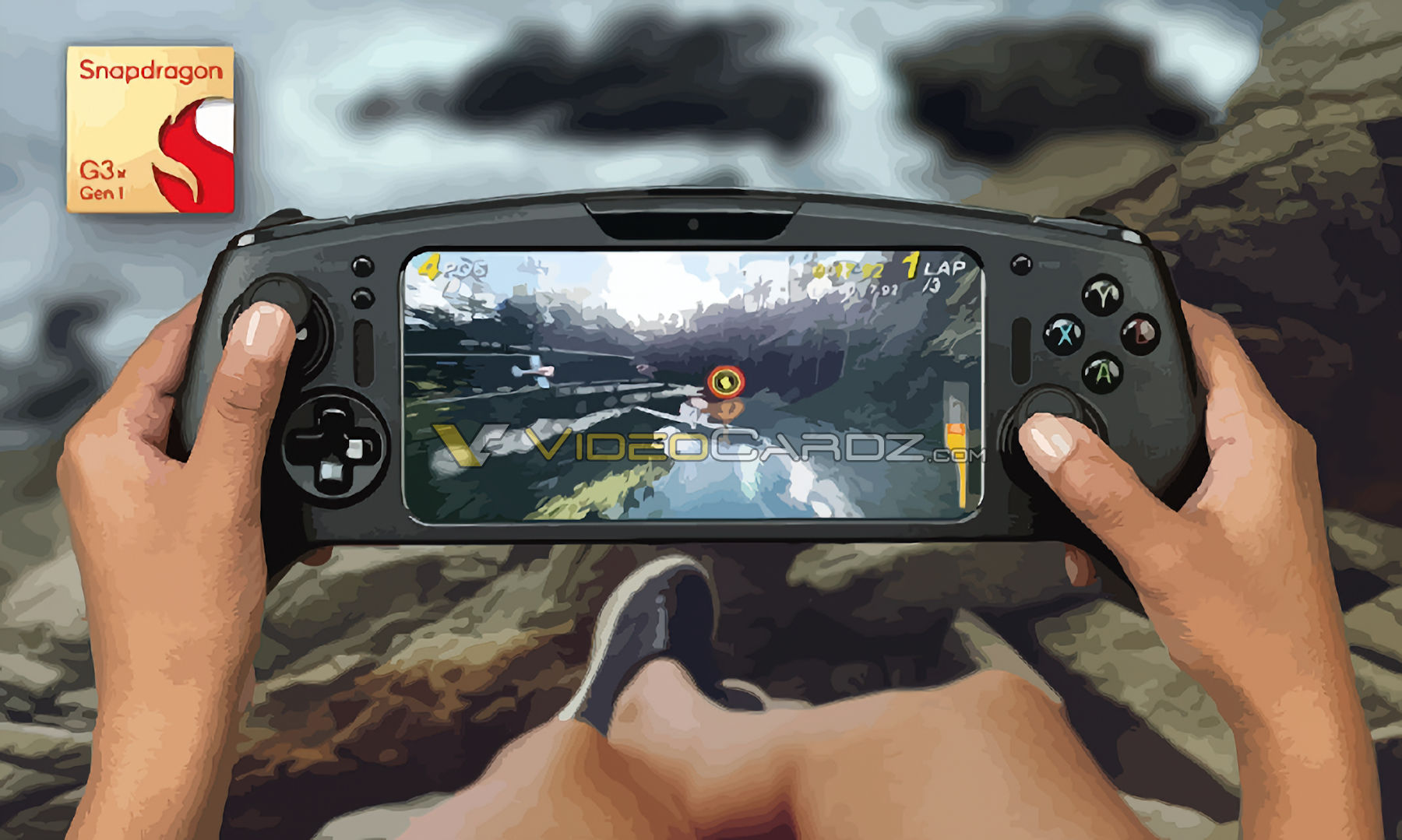
Qualcomm and Razer develop a Developer kit for next-gen mobile gaming The device, which is a Developer Kit, is powered by Snapdragon G3x silicon. We received a few slides featuring Qualcomm’s upcoming Snapdragon SoCs for 2022 products, including the G3x which was designed specifically for a...
This site uses cookies to help personalise content, tailor your experience and to keep you logged in if you register.
By continuing to use this site, you are consenting to our use of cookies.