• Hey everyone, staff have documented a list of banned content and subject matter that we feel are not consistent with site values, and don't make sense to host discussion of on Famiboards. This list (and the relevant reasoning per item) is viewable here.
  • Furukawa Speaks! We discuss the announcement of the Nintendo Switch Successor and our June Direct Predictions on the new episode of the Famiboards Discussion Club! Check it out here!

StarTopic Future Nintendo Hardware & Technology Speculation & Discussion |ST| (New Staff Post, Please read)

Where have you seen any evidence that they're being run more "committee-like"? From everything I've seen they appear to be following the same tenets set out during the Iwata era.

Labo and Ring Fit wouldn't be okayed by a committee of suits.
There were numerous articles about how inside of Nintendo, the culture has slightly changed. I dunno if its simple heresay or just speculation. Wish I had links to said articles off the top of my head...
 
There were numerous articles about how inside of Nintendo, the culture has slightly changed. I dunno if its simple heresay or just speculation. Wish I had links to said articles off the top of my head...
Yeah I don't remember reading or hearing about anything like that.
 
0
3rd-parties are very important to Nintendo(To the point they even change some hardware specifications due to feeback) and their share have been rising on Switch, but yeah. They wouldn't change architectures because developers asked them and frankly, that was just baseless conjecture from my part, as no developer would ask for that anyway.
I hope you realize how much of a non-statement this is.

I don’t want my tone to come off combative, but I don’t know how else to say it. So read this with a smile:

Nintendo is a platform, and like all platforms, they care about their people that make them money, in this case, 3rd party developers. But that’s like saying Facebook cares about ad spend. The difference is ~50% of units are Nintendo 1st party, and that translates into >70% of software sales.

Bringing up that Nintendo (probably) increased the memory due to feedback from Capcom (IIRC) is not comparable to picking an architectural. That’s more like Nintendo picking what kind of bridge they want to build and Capcom asking for an extra support beam.
 
To be fair, none of the first parties would listen to the third parties if they asked for a certain vendor. Third parties also don't really ask for that really, since they know they won't be listened to. It's a very, very, very big ask and they have to have a certain degree of audacity to ask that and expect it to happen.

Yes Microsoft and Sony are more third party driven than Nintendo, but none of the three would comply for a thing like that. It's far too complex of a business decision to do something like that and the only input third parties have into the hardware is what do they need from the first party hardware to have their engine support. Things like a stronger cpu, gpu, faster storage, more ram(always an ask), etc.


Something I assume third parties expect is to have the development environment be as good as possible regardless of the hardware they are given, ie they are given all the resources like documentation and whatnot for the hardware they are working with to know what they are doing to said hardware and how to achieve it.


And any modifications they do to the hardware would be things that are feasible without causing too much of an issue or delays, so clock speeds can be modified, amount of ram is not as rigid, but other than that the hardware is pretty much done and can't really be messed with too much on an architectural level.
 
0
I remember back in the NeoGaf days people were watching the costs spending of Nintendo research and development to see if they started spending for new hardware which was later revealed to be the NX/Nintendo Switch. I seen that Nintendo has now spent a billion in this department recently so is that a sign that the Nintendo Switch successor is already being assembled and worked on?
 
third parties won't even ask for vendors since software development has converged. there won't be a significant difference in developing for AMD or Nvidia outside of software and bonus hardware features, and there's not a significant difference in developing for x86/ARM (in a macro sense). all devs care about is enough memory, enough speed, and enough cores
 
I remember back in the NeoGaf days people were watching the costs spending of Nintendo research and development to see if they started spending for new hardware which was later revealed to be the NX/Nintendo Switch. I seen that Nintendo has now spent a billion in this department recently so is that a sign that the Nintendo Switch successor is already being assembled and worked on?
As for mass production, not necessarily, since I don't think mass production requires planning as far in advance as with chip development. But as for working on new hardware, definitely, especially with how much research goes into new hardware.
 
Only reason Nintendo would go with AMD is if Orins gaming performance is subpar. Reading rumors that the next Nvidia GPU’s are really thirsty ( low end needs a whopping 450w power supply) doesn’t bode well for that
In addition to what's already been stated, it's worth keeping in mind that a lot of Nvidia's recent GPUs have also been shipping with some pretty power hungry VRAM on the higher end, which is going to skew the numbers a bit.
 
0

What's interesting to me is that the dual benefits Intel gets from this, on one hand, you get the fastest process in the industry currently, on the other hand, Intel's forced to adopt these industry standard tools and approaches, which Intel's talked about before, but now you have no choice if you're going to be modular. You can't lean on integration and figuring out stuff in partnership with manufacturing, but that also feels like a really good wake up call for manufacturing because they can't get the design team to bend to their will if it's an external customer, and now they can't get it to do it if it's an internal customer either. Or is this too much searching for a silver lining in what is a bit of a suboptimal situation where you’re having to outsource and these sorts of things?

PG:
No, it's not. It is part of my conscious strategy, because I have one slide in my deck that says IDM makes IFS better and IFS makes IDM better.

This is one piece of that. Some of the things I said is, "Hey, IDM makes IFS better. Hey, it gets to inherit $10 billion of R&D for essentially free at that level". Huge capital outlays, et cetera, are enabling IFS, but IFS makes IDM better as well for exactly the reasons you're describing. I don't have to benchmark my TD team, my IFS customers are doing that for me. Some of these conversations, Ben, I just find them delightful. We have these five whale customers that we've talked about, these are active conversations. Active, daily things and in that, the teams are now saying, well, what about the ultra low voltage threshold for the thin pitch library that we're going to use in this particular cell? "TSMC is giving us these characteristics, you don't characterize that corner." Okay, guess what? Go characterize the corner! "Your PDK isn't as robust as the Samsung or TSMC PDK is to describe the process technology for my team to simulate." Well, guess what? You know, all of these things describe in conversations that make my TD team better, make my design teams more productive because they would've pushed on my TD team before to say, "Hey, we need that thin cell library at low voltage", and they wouldn't have gotten it.
Right.

PG:
Because it wasn't mainstreamed in the processor. It was sort of, "Hey, for some of these use cases over here". Well, now they get it, and all these things are driving us to be better. So in some ways, in a not very subtle manner, I've unleashed market forces to break down some of the NIH of the Intel core development machine, and that is part of this IFS making IDM better.

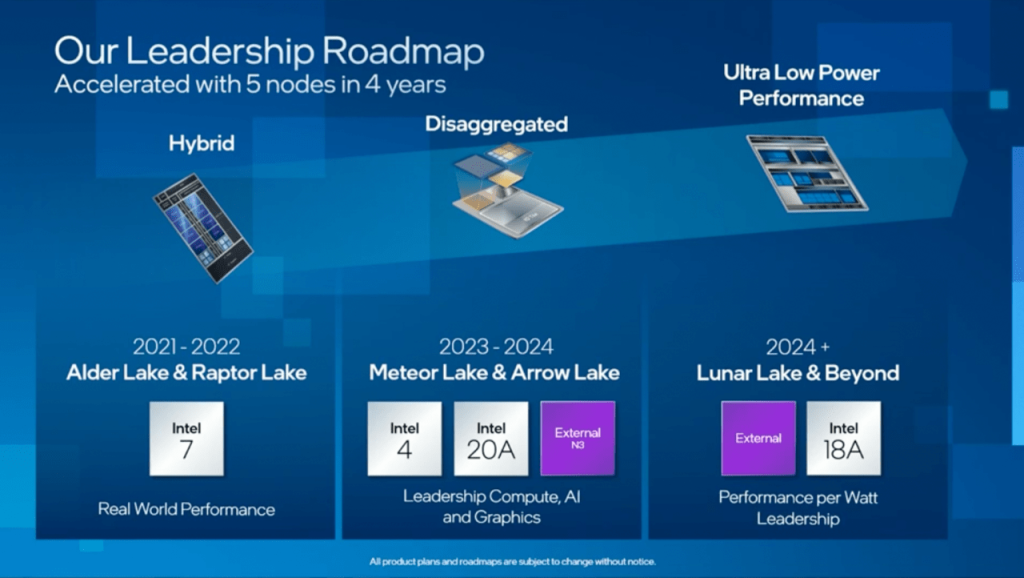
Yeah, that makes a lot of sense. You had this uber-aggressive roadmap, five nodes in four years, and I have two questions on that. The first one goes back to something you mentioned before about Apple being a partner to TSMC in getting to that next node and how important that was for TSMC. I think I noted that in this new Tick-Tock strategy, Tick-Tock 2.0, Intel's playing that role where either the tick or the tock is Intel pushing it and then the tock is opened up to your customers. I take it that's an example of how Intel being the same company really benefits itself, that you get to play the Apple role that Apple did for TSMC, you just get to play it for yourself.

PG:
Yeah, well stated. Now let's say, because I'm expecting Intel 18A to be a really good foundry process technology — I'm not opposed to customers using 20A, but for the most part, the tick, that big honking change to the process technology, most customers don't want to go through the pain of that on the front end. So usually my internal design teams drive those breakthrough painful early line kind of things, is very much like the Apple role that TSMC benefited from as well. Now, if Apple would show up and say, "Hey, I want to do something in 20A", I'd say yes.

Come on in!

PG:
If you list them, there are ten companies that can play that role — Qualcomm, Nvidia, AMD, MediaTek, Apple, that are really driving those front end design cycles as well, and if one of them wanted to do that on Intel 4, I'd do it, but I expect Intel 3 will be a better node for most of the foundry customers, like Intel 18A will be a better node for most of the foundry customers as well.
I think it's just Apple, and I think that's actually one of the powerful reasons for Intel to do this itself, and also frankly it's beneficial for TSMC to have Intel onboard as well as a counterweight.

One other thing, is it kind of nice in a way to be in second place? You've really emphasized a ton about how you are learning from and benefiting from your suppliers in a way that Intel didn't previously and I do want to dive into that a little bit more. Those suppliers have learned a lot from TSMC and from Samsung — how much of a role does your confidence that you can get learnings from your suppliers, drive your confidence that you can actually achieve this super aggressive rate of advancement?

PG:
It's a meaningful benefit. My team doesn't like the idea of being second in the race, so they’re pretty passionate. We do believe at 18A we're unquestionably back in the leadership role but getting EUV healthy on Intel 4, as an example, is very much benefited by the fact that TSMC and ASML have already driven that up the learning curves as well. I'm just asking ASML, "Are my layers per day on EUV, are they competitive?" Period. And if not, why not? I'd say we have very robust debates on those kind of questions now. "Well, they're measuring it differently than we measure it" and "How do you measure downtime and maintenance windows and all that kind of stuff" and I'm like, "Hey, I don't care. Just show me the fricking data." And you know, I go to Peter [Wennink] and Martin [van den Brink] at ASML and ask "How are we doing"? Or Gary [E. Dickerson] at Applied Materials and it just takes a lot of these things off the table, cracking open these doors just forces us to accelerate the competitiveness.

Yeah, I think getting Intel to drop the "They're measuring it differently" excuses is a win in and of itself.

PG:
(laughing)


Interesting to hear that Pat Gelsinger isn't opposed to customers, especially customers such as Nvidia, etc., using "tick" process nodes (e.g. Intel 4, Intel 20A). I wonder if Nvidia could actually ask to secure capacity for "tick" process nodes.
I seem to have forgotten to include this tidbit, which I find very interesting.
The Tower acquisition makes all kinds of sense to me in that Intel didn't need to just flesh out its portfolio of offerings that it had as a foundry, particularly in analog, but also needs to build out the capability of servicing external customers. This is a reason why I was cheering for an Intel GlobalFoundries tie-up at some point. Obviously, they don't have leading edge, but to your point, they've spent 14 years figuring out how to service external customers and building the IP around that, all those sorts of things. Tower does address some of those needs, my concern though is it’s much smaller in comparison to Intel, so how do you capture the parts of the customer service bit that you need without it being squashed by the Intel culture?

PG:
Is Tower being merged into Intel Foundry or is Intel Foundry being merged into Tower?

Right.

PG:
The answer is more the latter than the former. I've said I fully want to merge these businesses together going forward, and that doesn't mean this is a little satellite under this thing that we're getting started in IFS. We're going to bring those together, and I fully expect that the outcome is a fully integrated business unit that heavily leverages the five thousand people in Tower. Its thirty years old, Israeli-centered, and we know a lot about having good Israeli discipline as part of our team.

The other thing I’ve said is that, "Hey, I'd like to do a Mobileye-like spin on our foundry business at some point as well." I'm going to keep the structure, as opposed to integrating as much, I'm going to keep it more separate to enable that, which means I'm going to leverage a lot more of Tower and the expertise that it builds over time as part of it.

It was also interesting the contrast with GlobalFoundries, and I mean, I was interested in exploring GF. When we looked at Tower, it became apparent that there was a more natural fit here than first meets the eye. One of them is, "Hey, that would've cost me $30 billion, this will cost me $5.5 billion —"

all devs care about is enough memory, enough speed, and enough cores
Assuming 128-bit is the minimum memory bus width for Dane, I wonder if third party developers, such as Capcom for example, would request Nintendo to increase the memory bus width (e.g. from 128-bit to 192-bit, or from 128-bit to 256-bit) to increase the amount of memory bandwidth available for game development.
 
Yeah now that they know the Switch formula is a success and want to keep third party support coming, hopefully Nintendo doesnt cheap out on the memory bandwith or storage
 
I just got done watching Digital Foundry Steam Deck review and i wonder will the Dane be able to compete with it as well
Does it need to?
We're back to the power struggle wars again... I honestly don't think Dane is going to match a Deck in sheer horsepower, but will probably use DLSS to cheat itself in the rendering category.
 
Does it need to?
We're back to the power struggle wars again... I honestly don't think Dane is going to match a Deck in sheer horsepower, but will probably use DLSS to cheat itself in the rendering category.

I expect I’ll be equally or more impressed with Dane if they pull off PS4 visuals in handheld without any changes in device size or battery life.
 
I expect I’ll be equally or more impressed with Dane if they pull off PS4 visuals in handheld without any changes in device size or battery life.

Steam Deck is already a tad more powerful than Xbone. It doesn’t reach what the PS4 can do at 1080p.

I really don’t get it why it’s getting said that is a portable PS4 when it’s closer to a Xbone at 800p
 
Steam Deck is already a tad more powerful than Xbone. It doesn’t reach what the PS4 can do at 1080p.

I really don’t get it why it’s getting said that is a portable PS4 when it’s closer to a Xbone at 800p
*when it’s running the windows version through proton.

Just saying, a hypothetical well optimized steam deck game would blow minds.
 
I seem to have forgotten to include this tidbit, which I find very interesting.


Assuming 128-bit is the minimum memory bus width for Dane, I wonder if third party developers, such as Capcom for example, would request Nintendo to increase the memory bus width (e.g. from 128-bit to 192-bit, or from 128-bit to 256-bit) to increase the amount of memory bandwidth available for game development.

128-bit memory bus should definitely be more than enough for Nintendo to render at native 1080p resolutions and especially if they possibly go with Lpddr-5X instead of Lpddr-5. I personally still think that some sort of Nvidia Infinity Cache solution is the better way to go and we shall see once both Lovelace and RDNA3 both end up on TSMC's 5nm (later this year) of how efficient AMD's method is over Nvidia...
Is it fair to assume that Dane will be sub Steam Deck in terms of capabilities in handheld, but above it in docked, even before DLSS?
The thing that Dane will have over Steamdeck is developers being able to code much closer to the metal.
That alone will showcase games and a performance level on the system (unlike the Steamdeck) that can benefit from games using every aspect of the hardware features. Digital Foundry did some comparisons to PS4 and the architecture alone should net the Steamdeck better performance, but those same games being optimized and coded for PS4 hardware just performs better at a higher resolution.
 
Last edited:
I do believe the DLSS model* could be comparable with the PlayStation 4 in handheld mode, especially after DLSS is enabled.
 
I seem to have forgotten to include this tidbit, which I find very interesting.


Assuming 128-bit is the minimum memory bus width for Dane, I wonder if third party developers, such as Capcom for example, would request Nintendo to increase the memory bus width (e.g. from 128-bit to 192-bit, or from 128-bit to 256-bit) to increase the amount of memory bandwidth available for game development.
I just got done watching Digital Foundry Steam Deck review and i wonder will the Dane be able to compete with it as well
The OG switch was able to take it fairly well (25.6 GB/s) in regards to ports shared with xbone and PS4 in which the latter have a much bigger bandwidth (+100 GB/s). I though Nvidia tech knows how to use bandwidth really well? Newer Nvidia technology should be even more efficient than Maxwell when it comes to taking advantage of bandwidth.

I think 102 GB/s, plus increased cache on Orion is more than enough to play ps4 ports with similar performance (or better, along with GPU and CPU) at 1080p.
 
Steam Deck is already a tad more powerful than Xbone. It doesn’t reach what the PS4 can do at 1080p.

I really don’t get it why it’s getting said that is a portable PS4 when it’s closer to a Xbone at 800p
huh what. But it's using an 800p screen. Which can be docked in a 1080p screen. SD's CPU is way more powerful than the jaguars, and the GPU at 1.6 TFLOPs is much more newer and efficient and powerful than 2011 GCN GPU. Shouldn't have a problem out performing base PS4.
 
huh what. But it's using an 800p screen. Which can be docked in a 1080p screen. SD's CPU is way more powerful than the jaguars, and the GPU at 1.6 TFLOPs is much more newer and efficient and powerful than 2011 GCN GPU. Shouldn't have a problem out performing base PS4.
the issue is power limits. it caps at 15W. there's probably a way to exceed that
 
128-bit memory bus should definitely be more than enough for Nintendo to render at native 1080p resolutions and especially if they possibly go with Lpddr-5X instead of Lpddr-5.
My question is would a memory bus width of 128-bit be enough for third party developers, which is why I've mentioned third party developers in the original post.
 
My question is would a memory bus width of 128-bit be enough for third party developers, which is why I've mentioned third party developers in the original post.
Who cares? By the time this thing comes out, they will all have been bought up anyway.

Half serious.
 
Who cares? By the time this thing comes out, they will all have been bought up anyway.

Half serious.
Haha.

But to be fair, memory bandwidth's one of the biggest bottlenecks with the Nintendo Switch; so I think memory bandwidth is definitely one of Nintendo's biggest priorities when talking to Nvidia about Dane's design.
 
Haha.

But to be fair, memory bandwidth's one of the biggest bottlenecks with the Nintendo Switch; so I think memory bandwidth is definitely one of Nintendo's biggest priorities when talking to Nvidia about Dane's design.
I agree. However, memory bandwidth is one of those contstraints your just going to have to live with when it comes to portable hardware. So I don’t expect them to be able to fully alleviate that bottleneck.

But Orin having a lot more cache will certainly help.
 
the issue is power limits. it caps at 15W. there's probably a way to exceed that
I thought it can reach 1.6 TFLOPs GPU at 15 watts? Not expecting max CPU clocks to run with max GPU clocks at 15.. Is it at 1 TFLOPs or something?

Anyway I just read the article version of the video. Pretty interesting. I thought I heard some games running on better settings (ultra) with similar or better performance in performance than last gen consoles..

Will be interesting to see how they perform on a dock at 1080p vs PS4 base
 
My question is would a memory bus width of 128-bit be enough for third party developers, which is why I've mentioned third party developers in the original post.
I think for PS4 level based games/porte if shouldn't be an issue in theory. Maybe just for ports of current gen. But we also have increased cache from Orion, and DLSS as well t help...
 
0
I thought it can reach 1.6 TFLOPs GPU at 15 watts? Not expecting max CPU clocks to run with max GPU clocks at 15.. Is it at 1 TFLOPs or something?

Anyway I just read the article version of the video. Pretty interesting. I thought I heard some games running on better settings (ultra) with similar or better performance in performance than last gen consoles..

Will be interesting to see how they perform on a dock at 1080p vs PS4 base
I guess the issue is that the cpu and gpu can fight over those 15W. the 1.6TFLOPs is assuming the gpu gets the lion's share. DF shown that even a ps4 game like Days Gone can slow the game to a crawl due to cpu limitations
 
I guess the issue is that the cpu and gpu can fight over those 15W. the 1.6TFLOPs is assuming the gpu gets the lion's share. DF shown that even a ps4 game like Days Gone can slow the game to a crawl due to cpu limitations
Steam Deck's CPU is a current gen console equivalent CPU with half the cores. Doesn't need to be at 3Ghz to run circles around jaguars for PS4 ports..

does the steam deck have set GPU and CPU profile configurations at 15 watts and less?
 
I seem to have forgotten to include this tidbit, which I find very interesting.


Assuming 128-bit is the minimum memory bus width for Dane, I wonder if third party developers, such as Capcom for example, would request Nintendo to increase the memory bus width (e.g. from 128-bit to 192-bit, or from 128-bit to 256-bit) to increase the amount of memory bandwidth available for game development.

I'd argue that 128-bit is the maximum memory bus width for Dane, and by the time third party developers are able to give feedback, it's likely far too late to change it (unlike the quantity of RAM, which is just swapping out standardised components and could in theory be done a few months before launch). Besides, the limit on bus width isn't just physical space or cost, although they're not trivial, it's power consumption.

It's difficult to find hard numbers on RAM power consumption, but these Micron slides (PDF link) suggest LPDDR4 consumes about 6.5 Pj/bit, and the graph in this article (sourced from Samsung) indicates LPDDR5 consumes about 37.5% less power per bit than LPDDR4, so that would put LPDDR5 at just over 4 Pj/bit. Going to a 256 bit bus width at the full 6400MT/s would therefore consume over 6.5W for memory alone, which is a huge amount for a device like the Switch (by these numbers the original model maxed out at around 1.33W for 25.6GB/s). Even with a 128 bit bus, they're still looking at around 3.3W for the RAM at peak clocks, and will likely have to clock the memory down significantly in handheld mode. It's notable that even the Steam Deck, which has much higher power consumption than Switch, limits its LPDDR5 to 5500MT/s, and I'd imagine power consumption played a part in that decision.

Fortunately there's a more efficient approach, which is to rely more heavily on caches. I don't mean "infinity cache" (which is just marketing speak for a really big cache), but just generally bigger caches than you'd usually get on a chip like this. Accessing data in cache is far, far more power efficient than accessing data from off-chip DRAM, so if you want to maximise performance within a tight power budget, then big caches and a narrow memory bus is a better approach than small caches and a wide bus. Orin is moving in that direction, with 50% higher L1 cache on the SMs vs desktop Ampere, and a 4MB L2, and then another 4MB system-level cache above both the CPU and GPU. Dane won't have the same amount of L2, and probably not the SLC, but it's an indication that they're taking the right approach. The TX1 GPU only has 24KB of L1 cache per SM and a 256KB L2 cache, so even moving to 192KB L1 per SM and perhaps 1MB L2 would be a big jump.
 
Last edited:
huh what. But it's using an 800p screen. Which can be docked in a 1080p screen. SD's CPU is way more powerful than the jaguars, and the GPU at 1.6 TFLOPs is much more newer and efficient and powerful than 2011 GCN GPU. Shouldn't have a problem out performing base PS4.
From DF tests, its a bit above PS4 at 800p, but bellow at 1080p, probably due to memory bandwidth.
 
I'd argue that 128-bit is the maximum memory bus width for Dane, and by the time third party developers are able to give feedback, it's likely far too late to change it (unlike the quantity of RAM, which is just swapping out standardised components and could in theory be done a few months before launch). Besides, the limit on bus width isn't just physical space or cost, although they're not trivial, it's power consumption.

It's difficult to find hard numbers on RAM power consumption, but these Micron slides (PDF link) suggest LPDDR4 consumes about 6.5 Pj/bit, and the graph in this article (sourced from Samsung) indicates LPDDR5 consumes about 37.5% less power per bit than LPDDR4, so that would put LPDDR5 at just over 4 Pj/bit. Going to a 256 bit bus width at the full 6400MT/s would therefore consume over 6.5W for memory alone, which is a huge amount for a device like the Switch (by these numbers the original model maxed out at around 1.33W for 25.6GB/s). Even with a 128 bit bus, they're still looking at around 3.3W for the RAM at peak clocks, and will likely have to clock the memory down significantly in handheld mode. It's notable that even the Steam Deck, which has much higher power consumption than Switch, limits its LPDDR5 to 5500MT/s, and I'd imagine power consumption played a part in that decision.

Fortunately there's a more efficient approach, which is to rely more heavily on caches. I don't mean "infinity cache" (which is just marketing speak for a really big cache), but just generally bigger caches than you'd usually get on a chip like this. Accessing data in cache is far, far more power efficient than accessing data from off-chip DRAM, so if you want to maximise performance within a tight power budget, then big caches and a narrow memory bus is a better approach than small caches and a wide bus. Orin is moving in that direction, with 50% higher L1 cache on the SMs vs desktop Ampere, and a 4MB L2, and then another 4MB system-level cache above both the CPU and GPU. Dane won't have the same amount of L2, and probably not the SLC, but it's an indication that they're taking the right approach. The TX1 GPU only has 24KB of L1 cache per SM and a 256KB L2 cache, so even moving to 192KB L1 per SM and perhaps 1MB L2 would be a big jump.

We just need to get a magic wand to wave so to don't need to refresh the ddr 16 times a second and our power troubles will be gone.

Or make ddr retention longer than 64 Ms.

Basically I just want magic, I'm ready for technomancy.
 
0
Say, being a PC and all, can't one go into BIOS with the Steam Deck and edit power limits for the APU? Or is it hard locked down like certain vendors do with their laptops?
Valve just limited it, I’m pretty sure that just loading the BIOS and changing a few configs can let it go higher.

Like the RAM can be altered to operate at full.

But the power draw…. High.
 
0
Does anyone know if the Switch Pro is rumored to have exclusive games still? I know that was a big talking point back on Era for some.
 
I'd argue that 128-bit is the maximum memory bus width for Dane, and by the time third party developers are able to give feedback, it's likely far too late to change it (unlike the quantity of RAM, which is just swapping out standardised components and could in theory be done a few months before launch). Besides, the limit on bus width isn't just physical space or cost, although they're not trivial, it's power consumption.

It's difficult to find hard numbers on RAM power consumption, but these Micron slides (PDF link) suggest LPDDR4 consumes about 6.5 Pj/bit, and the graph in this article (sourced from Samsung) indicates LPDDR5 consumes about 37.5% less power per bit than LPDDR4, so that would put LPDDR5 at just over 4 Pj/bit. Going to a 256 bit bus width at the full 6400MT/s would therefore consume over 6.5W for memory alone, which is a huge amount for a device like the Switch (by these numbers the original model maxed out at around 1.33W for 25.6GB/s). Even with a 128 bit bus, they're still looking at around 3.3W for the RAM at peak clocks, and will likely have to clock the memory down significantly in handheld mode. It's notable that even the Steam Deck, which has much higher power consumption than Switch, limits its LPDDR5 to 5500MT/s, and I'd imagine power consumption played a part in that decision.

Fortunately there's a more efficient approach, which is to rely more heavily on caches. I don't mean "infinity cache" (which is just marketing speak for a really big cache), but just generally bigger caches than you'd usually get on a chip like this. Accessing data in cache is far, far more power efficient than accessing data from off-chip DRAM, so if you want to maximise performance within a tight power budget, then big caches and a narrow memory bus is a better approach than small caches and a wide bus. Orin is moving in that direction, with 50% higher L1 cache on the SMs vs desktop Ampere, and a 4MB L2, and then another 4MB system-level cache above both the CPU and GPU. Dane won't have the same amount of L2, and probably not the SLC, but it's an indication that they're taking the right approach. The TX1 GPU only has 24KB of L1 cache per SM and a 256KB L2 cache, so even moving to 192KB L1 per SM and perhaps 1MB L2 would be a big jump.
Couldn’t Nintendo ask Nvidia to add more cache or keep the same amount as the big Orin has? Or would that simply cost too much on Nintendo’s end?
 
I don't get it.. there's been Nvidia graphics cards with 50 GB/a bandwidth that were going toe to toe with xbone and PS4 games.. And they were from the Turing age I believe..
I believe the particular cases we are referreing to are horizon and god of war. Extremely well optimized first party ps4 games, vs windows versions running through proton.

I’m sure many games performs better on SD.
 
Couldn’t Nintendo ask Nvidia to add more cache or keep the same amount as the big Orin has? Or would that simply cost too much on Nintendo’s end?
Theoretically speaking, yes to the former. As for the latter, cost's not the only factor. More cache also at the very least considerably increases the die size (i.e. Infinity Cache).
 
Theoretically speaking, yes to the former. As for the latter, cost's not the only factor. More cache also at the very least considerably increases the die size (i.e. Infinity Cache).

ok, hopefully if they go with more cache it doesn’t get too big so they have to cut down on something else
 
0
Couldn’t Nintendo ask Nvidia to add more cache or keep the same amount as the big Orin has? Or would that simply cost too much on Nintendo’s end?
I'm sure Nintendo have discussed cache requirements for Dane with Nvidia, but keeping the same amount of L2 as Orin would be a big ask, due to the die size (and therefore cost) of it. We can look at the GA102 die, for which there's a nice large annotated die shot here, as a point of comparison. It has 6MB of L2 cache (for 84 SMs), split into two 3MB blocks on the die. We can calculate the size of these from the die shot (knowing the full die is 628.4mm2), with a single 3MB block of L2 coming in at 22.1mm2. For 4MB, therefore we would be looking at about 29.5mm2. That's a full quarter of the die area of the original TX1.

Of course it's not impossible for Nintendo to allocate a large die area to memory, they've done it before with the Wii U, but there's also diminishing returns to ever larger caches (and increased latency as the cache grows, although that's likely to be less of an issue on the GPU side). If they had a 1MB L2 GPU cache, with 4 SMs that would put them at 3.5x as much L2 cache per SM as GA102. Even at the upper end of people's expectations here, with 8 SMs it would still be significantly more cache per SM than desktop Ampere. For comparison, TX1 had the same L2 per SM as desktop chips like GM204 (128KB per SM).
 
I do think Nintendo could use more power with Dane, batteries have become more dense over the past 5 years and I still think joycons could offer their batteries to increase capacity and battery life when on the go. When docked, they could pull much more than they did for the Switch, the form factor isn't quite as limited and Nintendo has much more room to mm^2 to work with than Valve, as Valve's components are entirely off the shelf and much less integrated than Nintendo has been with the Switch. It's actually quite cramped inside of a steamdeck, given the vastly larger casing than Switch.
 
Last edited:
Right, Gamers Nexus clocked the Steamdeck at up to 30 watts for demanding games for total system draw on the battery.

I remember reading something like that in the Eurogamer article 🤔. That does change things quite a bit in terms of what we could expect for switch 2.

I wonder what the exact GPU and CPU clocks were to reach those. Clearly they reached the past the threshold, so the the power consumption sky rocketed.
6-8 A78 cores at up to 1.5GHz should consume less power than 4 Ryzen CPU cores at 2.5-3Ghz total, right?

30 watts at 1.5 hrs is not bad though for demanding games on steam deck.

I hope Nintendo goes over 15 watts.. l like 25 watts docked. Maybe then it could reach similar performance to steam deck, but in docked mode with lower CPU performance.

I guess something like a 5nm TSMC chip really is needed for comfortable handheld PS4 performance. That might be doable for 15 watts for the whole system 🤔. But we'll likely have to wait for a revision for that.
 
Last edited:
I remember reading something like that in the Eurogamer article 🤔. That does change things quite a bit in terms of what we could expect for switch 2.

I wonder what the exact GPU and CPU clocks were to reach those. Clearly they reached the past the threshold, so the the power consumption sky rocketed.
6-8 A78 cores at up to 1.5GHz should consume less power than 4 Ryzen CPU cores at 2.5-3Ghz total, right?

30 watts at 1.5 hrs is not bad though for demanding games on steam deck.

I hope Nintendo goes over 15 watts.. l like 25 watts docked. Maybe then it could reach similar performance to steam deck, but in docked mode with lower CPU performance.

I guess something like a 5nm TSMC chip really is needed for comfortable handheld PS4 performance. That might be doable for 15 watts for the whole system 🤔. But we'll likely have to wait for a revision for that.
I don't think PS4 fidelity will take much. ARM A78 cores at 1.5GHz even 7 of them (for games and reserved 1 for OS at an independent clock) on 8nm would use FAR less energy than 4 Ryzen 2 cores at 3GHz on 7nm. If we take a quick look at Turing based MX550 that was recently announced, it uses GDDR6 (power hungry memory) on 12nm and still offers ~PS4 Pro level of fidelity with 25 watts. 8nm is a huge jump from 12nm, (around 33% reduction in power consumption) in terms of this GPU, if the RAM uses 10 watts and the GPU is using 15 watts, you'd see an 8nm version of this PS4 Pro level chip, consume up to 10 watts.

Ampere is more energy efficient per flop, though performance is lower per flop, it is also important to note that Orin and Dane have the extra cache (if Kopite7's comments about Ada lovelace are accurate). I'm suggesting a reduction of half the power consumption, which should result in ~2TFLOPs of Ampere performance on 8nm for up to 7 watts for just the GPU, in handheld the original Switch used almost 10watts, there is some room for more power consumption in the newer model, so they should have no trouble hitting original PS4 performance in handheld mode without even using DLSS in a power consumption similar to the original Switch. Thanks to features like FSR/NIS and DLSS, the portable mode could have longer battery life and still offer PS4+ fidelity on the go, while docking and pushing into PS4 Pro/XBSS performance.
 
Please read this new, consolidated staff post before posting.

Furthermore, according to this follow-up post, all off-topic chat will be moderated.
Last edited by a moderator:


Back
Top Bottom