If it's running on ARM, then it's not really a "PC handheld" anymore. The whole draw of something like the ROG Ally to a PC gamer is that it's the exact same as an equivalent PC under the hood with no architectural weirdness, and having to deal with x86 to ARM translation would add quite a bit of jank. So long as Nvidia doesn't have an x86 license and Intel continues to prioritize productivity in their CPU architectures, AMD will continue to dominate the handheld PC market.
Fair enough with the PC part. it's gonna be really interesting when they get a Nvidia GPU with an AMD or Intel CPU.
The GPU and the CPU on Deck don't run at max speed at the same time, they're power limited. The GPU gets priority.
Yeah I've heard that, but don't think I got answer on the exact speeds (and I did some searching) other than each other's on paper clock speeds (including SD's 2.4-3.5GHz range). Of course this is on a 15 watt TDP, and I'm guessing missing is required to go to higher, and requires like 25 watts total or something with less than an hour of battery life?
The max GPU speeds of 1.6GHz or 1.6 TFLOPs on on SD will always be the comparison point. In this case, if the CPU only goes 2.1-2.4Ghz when max GPU 1.6Gh, is enabled, Switch 2 should without a doubt, steam roll it in CPU performance, no? The Switch 2 is already anticipated to use 8 A78C cores (7 for gaming) at around 1.5-1.7GHz
Honestly kinda disappointed. It's still a technical marvel in it's own right as a handheld PS4 with 15 watts on 7nm TSMC (OG version). But it's just not how I imagined it. The power gap between it and the Series S is wider than I thought on the CPU front (outside of 3 vs 7 for gaming).
But it makes more sense now why it's the most efficient/powerful PC handheld at 15 watts when the CPU is only around 2GHz on 3 CPU cores with the GPU maxed , or when the GPU is as low as 1GHz when CPU are max clocks vs 8 AMD CPUs at higher clocks, despite using newer nodes like 5nm.
I wonder how SD OLED fares in power draw though in regards to max clocks.
it doesn't change much for that Switch 2 I guess. Better expected performance comparisons vs SD, nit against current gen, nothing changes.
I place very little faith into MLID's "sources", but I wouldn't be too surprised if 1.3GHz (and therefore 4 TFLOPS) was an internal target for Nvidia, even if they didn't expect Nintendo to clock it that high. Even if Nintendo had settled on, say 1.1GHz as a target clock in docked mode during the design process, the actual clock speed could end up lower or higher than that based on the performance of the silicon, other hardware design changes, etc., so there would want to be some wiggle room in achievable clocks to accommodate that. A 1.3GHz clock is probably a reasonable upper limit of what Nintendo may choose, and also a round number in both clock speed and Gflops, so it's a plausible target for Nvidia. Besides, every other Ampere GPU can clock well past 1.3GHz, so it's really quite a modest target for the architecture.
On the LPDDR5X side, I could see it happening for two reasons outside of performance requirements. The first is simply that Nvidia was already working on an in-house LDDDR5X controller (for Grace) with a similar tape-out timescale, and it may have been the case that using the updated controller would have a near-zero impact on cost and timelines, so it was basically the default option.
The second is availability of LPDDR5/X RAM down the line. Back when Nintendo and Nvidia started supporting LPDDR4X with Mariko, I assumed it was purely for the sake of the power efficiency benefit. This may have been partly the case, but in the years after release, LPDDR4 has all but disappeared from the market, with LPDDR4X almost completely replacing it. Being able to use a widely available (and therefore cheap) form of RAM for the rest of the console's life was likely a major reason behind switching from LPDDR4 to 4X.
With Switch 2, it seems pretty unlikely that there will be a Mariko-style updated SoC at any point in the console's lifespan, which means they'll need to design a system which they can still buy parts for perhaps as much as 8 years later. Nintendo (and, I'm sure Nvidia) have surely spent a lot of time talking with RAM manufacturers about the production lifespan of the parts they're interested in, and if it's expected that LPDDR5X will almost completely replace 5 in the same way 4X replaced 4, then there would be a very strong incentive for Nintendo to have an SoC with LPDDR5X support even if they had no intention of using the higher speeds.
I think a revision is definitely possible if Nintendo isn't happy with the battery life of Switch 2 on release, and if they think they will still gain the same profit (or more), or save $s on newer parts meant to extend the battery life.
Meaning..
1. If Switch 2 gets the same battery life as OG Switch at launch (3 hrs), a revision will happen. YES
2. If switch 2 battery life is closer to Mariko, maybe not.
When I say revision, I mean node revision with power draw savings. I don't think we'll get a big jump node like 20nm to 16nm, but I do think a 30-50% power savings is probably possible like Steam Deck OLED vs Steam Deck OG.
3nm node in 2029/ might save 20% on power draw and be mature enough to cost the same as 5nm does now, slap on an OLED screen, and a more newer and power efficient SSD, it can probably be done.
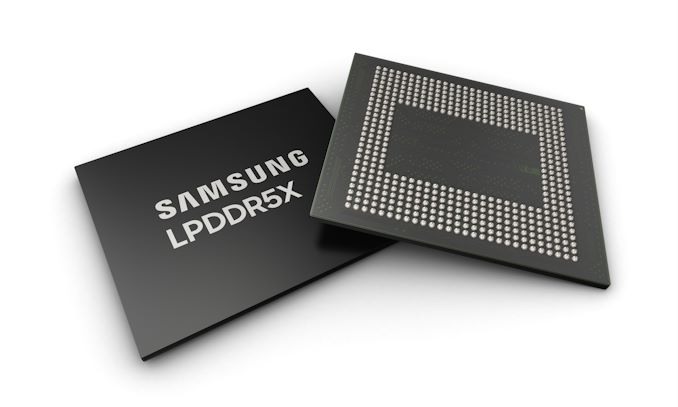
As for RAM... If we are lucky and manage to get lpddr5x--and with max speeds of 8533 Mbit/s (134GB/s) at launch, maybe for a 2029 revision we can get LPDDR5X-10700. Using a 12nm node process, it offers 25% more bandwidth.. or 25% power efficiency (I'm assuming at the same clockspeeds as a regular lpddr5x).. so .75 watts vs 1 watt

?
I don't know when the lpddr5x-10700 will be released. Maybe in late 2025

www.anandtech.com


 Normally Pyoro clarifies pretty quickly what their hints are related to, right? I don't know their usual posting hours, but I wonder if they're sleeping and that might be why. That always is a possibility. This thread's been going wildfire and I've been trying to catch up since I woke up, lol.