• Hey everyone, staff have documented a list of banned content and subject matter that we feel are not consistent with site values, and don't make sense to host discussion of on Famiboards. This list (and the relevant reasoning per item) is viewable here.

StarTopic Future Nintendo Hardware & Technology Speculation & Discussion |ST| (New Staff Post, Please read)

Business Description
Hardware and software development of inspection equipment used in mass production processes
  • Characteristic testing equipment for game console input/output devices
  • Inspection equipment for checking the operation of finished game console products
  • Inspection equipment for checking the operation of accessories for game consoles
Hm...for me in Chrome with Google Translate the translation for the middle bullet point is just "finished game consoles"...which is pretty damn smokey. "game console products" could obviously cover more things...things that would likely already be included in points 1 & 3 though. But yeah, even a game console doesn't have to be Drake I guess.

(maybe a Nintendo Gamecube Classic Edition...a little 4" cube would be kind of cute) /s
 
Yeah, that text in Japanese absolutely seems to refer to "finished product" testing for the systems and accessories in the second and third parts of the text. First part is vague enough but definitely related to the other two.

If nothing else, that seems like a good sign Nintendo's gearing up for a possible release sooner than later. It could still absolutely get pushed back if something happens (this phase goes wrong, manufacturing issues, etc.), but them hiring for testing the finalized system out is a good sign.
 
0
8nm still strikes me as significantly more likely than 7nm or 5nm, even if the chip is larger. Nintendo's generally not one to use bleeding-edge nodes.

It's not a coincidence that the PS5 and XSS/X adopted TSMC N7 in the same year Apple moved their latest products from TSMC N7 to TSMC N5, freeing up tons of 7nm capacity and making that node cheaper. I don't think any game system, especially a Nintendo one, is going to jump to N5 until Apple starts moving in a big way to N3, and it seems like a large portion of Apple's products this year are still going to be on N5.

It absolutely is a coincidence that PS5 and XBSS/X adopted N7 the same year Apple moved to N5. The decision would have been made perhaps three years prior to launch when design work began, without any knowledge of Apple's plans. The timing of the PS5 and XBSS/X launches were based on Sony and MS's product lifecycles, and the choice of N7 was an obvious one, as AMD had already been shipping consumer GPUs on TSMC 7nm for a year and a half by the time of the new console launches, and MS and Sony wanted to use the same RDNA/RDNA2 architecture.

Similarly, Nvidia aren't making the decision on what manufacturing process to use in 2022 based on what Apple's doing now, they made the decision perhaps in late 2019 or early 2020 based on the information they had at the time. At the time, they were confident enough about TSMC N5 (or 4N, as they're calling it) availability to migrate their entire line of GPUs (both Hopper HPC and Ada gaming GPUs) over to the process in a similar timeframe as we're looking at for Drake. These would account for at least an order of magnitude more wafers per month than Drake, so I can't see Nvidia not being confident enough to get the much smaller allocation necessary for Drake.

The other thing to emphasise is that Nintendo's not designing or manufacturing the chip, they're buying chips designed and manufactured by Nvidia, and therefore it's ultimately Nvidia's decision as to what manufacturing process to use. Obviously this decision isn't made in isolation, as it's a semi-custom design for Nintendo the choice of node would be made based on Nintendo's requirements for performance, cost and power consumption. If Nintendo's performance requirements weren't exactly pushing the envelope, then an older manufacturing process might make sense, and that what most of us were expecting prior to this month. However we now have very explicit details leaked from Nvidia showing a GPU which is absolutely pushing the envelope for performance in a Switch-style device. We also can reasonably estimate power consumption assuming a device with the same form-factor as the Switch, and it looks much more likely that Nvidia would have chosen TSMC N5 based on those requirements. It's also entirely possible that TSMC N5 is cheaper (perhaps substantially so) per chip than Samsung 8nm when taking die size and yields into account, in which case Nvidia would have no incentive to incur extra expense manufacturing on Samsung 8nm if they weren't forced to.

Finally, it's worth noting that if the new Switch model launches in March 2023, then TSMC's 5nm family will be exactly as old as 20nm was when Switch launched in 2017. If Nintendo were happy with that, I hardly see them being scared off of N5 as being too "bleeding-edge" for them.
 
Last edited:
That'd probably be for products expected to launch next year; mass production starts later this year then turns into shipping for revenue the beginning of next.
Yes. But more importantly is that Apple isn’t remaining on 5nm for the next few years like we think. They are planning to move on shortly even if Drake launched this year or next year so capacity should be opened up if it hasn’t already.


Business Description
Hardware and software development of inspection equipment used in mass production processes
  • Characteristic testing equipment for game console input/output devices
  • Inspection equipment for checking the operation of finished game console products
  • Inspection equipment for checking the operation of accessories for game consoles
This could easily just apply for the current switch fwiw. It’s why I don’t consider it as meaning anything tbh.
 
While it's still likely the case that Samsung 8nm has the best availability, I finally looked for the quote where Nvidia's CFO was leaving the door open for continued RTX 30 series production.
Nvidia's CFO having a Q&A session at a Morgan Stanley event on March 7
Relevant quote:
Joe Moore

Great. And then last gaming question, new products. I know you're going to tell me you can't talk about unannounced products. But to the extent that, I guess, you've got third generation ray tracing, you have an Ampere cycle that never really saw the demand completely satiated. Does that actually make it challenging a little bit in terms of transitioning from this product to the next one when you never were able to fill that? And am I right to think that third generation ray tracing is probably an important feature?

Colette Kress


So, we've always focused on exciting our gamers with every new generation that comes out or another way to think about that is, of course, we're working behind the scenes on what's coming up next. That's just something that we do. We believe in the best of breed that is when it's ready, we will bring it to market. That's about the best thing that we can do. And we always have gamers that are excited for each generation that comes out to be first to overall purchase that.


So, you're correct. We're not here to announce products. And I think you'll continue to hear us both talk about some items here at GTC as well as things going forward. But it doesn't -- nothing changes. And even during this period of COVID and supply constraint, it's been interesting because it's given us the opportunity for gaming to continue to sell both the current generation as well as the Turing generation. So we've been doing that to provide more and more supply to our gamers in that, and we may see something like that continue in the future. It was successful with Ampere, and we'll see as we move forward.

Nothing in stone, of course. It's just curiously coy.

Yes. But more importantly is that Apple isn’t remaining on 5nm for the next few years like we think. They are planning to move on shortly even if Drake launched this year or next year so capacity should be opened up if it hasn’t already.
Oh, certainly. If N3 gets up and running, someone's selling something next year from it (who else would it be other than Apple?).
 
I think the bigger line from the job posting is this:

-Experience in starting up mass production of electrical products

Why would Nintendo be looking for someone to help with starting up mass production of a product they already make?
 
I think the bigger line from the job posting is this:

-Experience in starting up mass production of electrical products

Why would Nintendo be looking for someone to help with starting up mass production of a product they already make?
Note that it could not really refer to a game console but could refer to an accessory that works with the game console


I’m coping hard here 🫠
 
Last edited:
This isn’t directly related to what you said, and while Digitimes is hit or miss with accuracy, it’s interesting that this is reported:


NV is definitely one of the three.

Speaking of 2nm, that should still be targeting 2025. Possible candidate for Atlan...

Intel could/should be one too. Looking at slides from the last investor meeting, for Meteor Lake & Arrow Lake (2023-2024), Intel 4, Intel 20A, and 'External N3'. Most likely it's the GPU tile being on the external node, and that should be Battlemage. 2024+ ('Lunar Lake & beyond') is planned to be using Intel 18A and 'External'. Probably Celestial that's being made externally. Interesting that 'External' doesn't have a number included; probably N2 but too early to be confident about it, I suppose.

Speaking of possibilities for Atlan though, the slides do present Intel 18A targeting being available as part of IFS in late 2024.
 
We knew the OLED was coming because leaked 6.99 inch screen purchase orders were made from Samsung(as early as January 2021, but confirmation was in March 2021) If we can find something similar again, then we would know for sure a new switch is on the way
 
0
Speaking of 2nm, that should still be targeting 2025. Possible candidate for Atlan...

Intel could/should be one too. Looking at slides from the last investor meeting, for Meteor Lake & Arrow Lake (2023-2024), Intel 4, Intel 20A, and 'External N3'. Most likely it's the GPU tile being on the external node, and that should be Battlemage. 2024+ ('Lunar Lake & beyond') is planned to be using Intel 18A and 'External'. Probably Celestial that's being made externally. Interesting that 'External' doesn't have a number included; probably N2 but too early to be confident about it, I suppose.

Speaking of possibilities for Atlan though, the slides do present Intel 18A targeting being available as part of IFS in late 2024.
Probably not for Atlan, it’s currently being sampled and it is using “Ampere Next” GPU as per NVidia’s slides. Which is most likely Ampere or Hopper in some capacity I think.

Edit: wrong year, it’s 2023 it gets sampled.

And I meant Lovelace, not ampere.
 
Last edited:
Note that it could not really refer to a game console but could refer to an accessory that works with the game console


I’m coping hard here 🫠
I can see your viewpoint, but then why would they list game consoles AND accessories?

  • Inspection equipment for checking the operation of finished game console products
  • Inspection equipment for checking the operation of accessories for game consoles

Maybe I'm misunderstanding the wording used (and I should note that it's translated through DeepL), but it sounds like this would be not only the new Switch itself, but also potentially new joycons and/or dock, correct?


On a separate note, how would Samsung 8nm vs TMSC 5nm change our expectations for this SoC? Would it mean everything would be improved (CPU/GPU, RAM, storage speed, etc.) or better battery life? How much better we talking percentage wise (size, efficiency, etc.)? I know that it's hard to compare flops across different vendors and architectures, but is it easy to directly compare Samsung 8nm vs TMSC 5nm?
 
I can see your viewpoint, but then why would they list game consoles AND accessories?

  • Inspection equipment for checking the operation of finished game console products
  • Inspection equipment for checking the operation of accessories for game consoles

Maybe I'm misunderstanding the wording used (and I should note that it's translated through DeepL), but it sounds like this would be not only the new Switch itself, but also potentially new joycons and/or dock, correct?
To sum up thinking from earlier in thread:
  • The inspection job is almost definitely for QA tools for an assembly line
  • The Circuit Design job seems to be for controller work
  • The three hardware jobs might not be related
  • And even if they are, they could be for a new Mini Console, or Non-Drake Revision
    • Nintendo has specifically said they are looking into internal redesigns of Switch that would reduce their need for various ASIC and make them less affected by the chip shortage
  • Or even just backfills
These hires are suggestive as hell but not definitive.
 
0
It absolutely is a coincidence that PS5 and XBSS/X adopted N7 the same year Apple moved to N5. The decision would have been made perhaps three years prior to launch when design work began, without any knowledge of Apple's plans. The timing of the PS5 and XBSS/X launches were based on Sony and MS's product lifecycles, and the choice of N7 was an obvious one, as AMD had already been shipping consumer GPUs on TSMC 7nm for a year and a half by the time of the new console launches, and MS and Sony wanted to use the same RDNA/RDNA2 architecture.

Similarly, Nvidia aren't making the decision on what manufacturing process to use in 2022 based on what Apple's doing now, they made the decision perhaps in late 2019 or early 2020 based on the information they had at the time. At the time, they were confident enough about TSMC N5 (or 4N, as they're calling it) availability to migrate their entire line of GPUs (both Hopper HPC and Ada gaming GPUs) over to the process in a similar timeframe as we're looking at for Drake. These would account for at least an order of magnitude more wafers per month than Drake, so I can't see Nvidia not being confident enough to get the much smaller allocation necessary for Drake.

The other thing to emphasise is that Nintendo's not designing or manufacturing the chip, they're buying chips designed and manufactured by Nvidia, and therefore it's ultimately Nvidia's decision as to what manufacturing process to use. Obviously this decision isn't made in isolation, as it's a semi-custom design for Nintendo the choice of node would be made based on Nintendo's requirements for performance, cost and power consumption. If Nintendo's performance requirements weren't exactly pushing the envelope, then an older manufacturing process might make sense, and that what most of us were expecting prior to this month. However we now have very explicit details leaked from Nvidia showing a GPU which is absolutely pushing the envelope for performance in a Switch-style device. We also can reasonably estimate power consumption assuming a device with the same form-factor as the Switch, and it looks much more likely that Nvidia would have chosen TSMC N5 based on those requirements. It's also entirely possible that TSMC N5 is cheaper (perhaps substantially so) per chip than Samsung 8nm when taking die size and yields into account, in which case Nvidia would have no incentive to incur extra expense manufacturing on Samsung 8nm if they weren't forced to.

Finally, it's worth noting that if the new Switch model launches in March 2023, then TSMC's 5nm family will be exactly as old as 20nm was when Switch launched in 2017. If Nintendo were happy with that, I hardly see them being scared off of N5 as being too "bleeding-edge" for them.

This was all that I wanted to get across when discussing possible nodes for this chip. That you and many others have provided links, charts, tweets and percentages to the community with valuable information just as a sounding board of why something like 5nm could be a possibility.

Nvidia running away from Samsung to pre-purchase capacity with TSMC at such a large sum of money also gives some credence to the company valuing not only TSMC's ability to meet capacity at good yields, but a much clearer roadmap for advanced process technology in the future as well (speculation of course on my part).
 
0
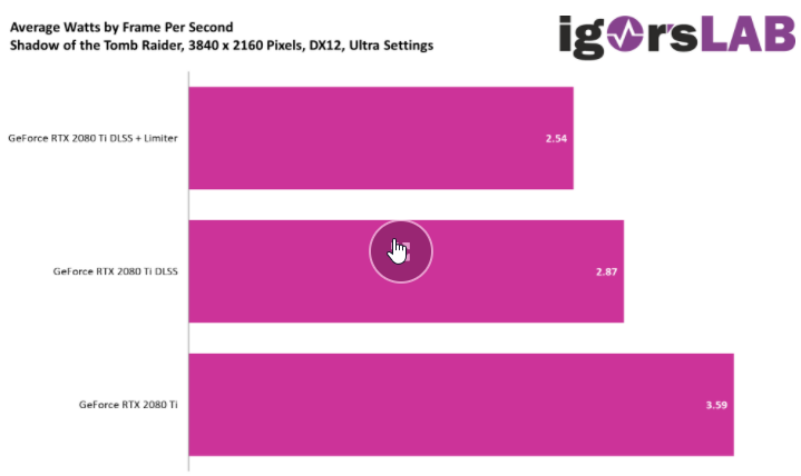
There is good news for those among us who want to see DLSS in portable mode. According to Igors' Lab experiment (I didn't know the source but the tests seem sensible), running Shadow of the Tomb Raider using DLSS actually saves energy per frame rendered:

2022-03-2510_39_16-wia0k73.png


In this example, the savings amount to 20% power on each frame. That is substantial when we consider what impact on the battery life this can have. It's not gargantuan mind you, but this might have caught Nintendo's attention.

I should say though that all the caveats regarding DLSS in handheld mode still apply: we have less power at disposal compared to docked mode and because of this, DLSS will likely eat up a lot of the time budget per frame. However, if it consistently saves up energy, then it can increase the likeliness of Nintendo trying to make it work.

And of course, the power savings would scale up in docked mode as well.
Well, there it is. Guess most games that really push the hardware will use DLSS in handheld. Hopefully they pick a good base resolution, going as low as 240p creates significant artifacting.
 
Quoted by: SiG
1
On a separate note, how would Samsung 8nm vs TMSC 5nm change our expectations for this SoC? Would it mean everything would be improved (CPU/GPU, RAM, storage speed, etc.) or better battery life? How much better we talking percentage wise (size, efficiency, etc.)? I know that it's hard to compare flops across different vendors and architectures, but is it easy to directly compare Samsung 8nm vs TMSC 5nm?
Thraktor's post here should cover estimates for transistor density/size.

Efficiency's hard to compare across foundries, exact percentage-wise. But to generalize:
Samsung 8nm is a further refinement of their 10nm node, and thus is part of the 10nm generation (going by ITRS).
The next generation is 7nm. For TSMC, the N7 family (including N6) is part of that. For Samsung, it's their 7nm through 5 nm nodes. Within that generation, TSMC's generally considered the more desirable option. I think that smartphone reviews have Samsung 5nm chips being less efficient than N7/N6 counterparts?
Continuing on, next generation is 5nm. For TSMC, it's the N5 family (including N4). For Samsung, it's their 4nm group of nodes... which were originally presented as further extensions of the 7-6-5 nm line, but then recently reclassified as a new generation :whistle:
TSMC is widely considered to be the winner of this generation. And since the 3nm generation hasn't kicked off yet, the N5 family is today's best.

But to be honest, I'm... actually unsure how Samsung 4nm compares to TSMC N7/N6, efficiency-wise.
 
I can see your viewpoint, but then why would they list game consoles AND accessories?

  • Inspection equipment for checking the operation of finished game console products
  • Inspection equipment for checking the operation of accessories for game consoles

Maybe I'm misunderstanding the wording used (and I should note that it's translated through DeepL), but it sounds like this would be not only the new Switch itself, but also potentially new joycons and/or dock, correct?


On a separate note, how would Samsung 8nm vs TMSC 5nm change our expectations for this SoC? Would it mean everything would be improved (CPU/GPU, RAM, storage speed, etc.) or better battery life? How much better we talking percentage wise (size, efficiency, etc.)? I know that it's hard to compare flops across different vendors and architectures, but is it easy to directly compare Samsung 8nm vs TMSC 5nm?
Accessories can apply to pretty much any new product related to the switch family, be it wristband, dock, things like Ring-Fit, etc. they don’t necessarily entail that is new product.

The Game console part could refer to the switch next, but only because the person who was there previously left so they are searching for a new person. It doesn’t mean it’s for something right imminent. The OLED model likely had one but the person left.

Basically I wouldn’t read to much into it (and maybe be led to disappointment :p)
 
Probably not for Atlan, it’s currently being sampled and it is using “Ampere Next” GPU as per NVidia’s slides. Which is most likely Ampere or Hopper in some capacity I think.
Sampling for Atlan actually hasn't started yet. Nvidia plans to sample Atlan in 2023, which is probably when Nvidia has to make the final decision on which process node is used, especially when taking into account the amount of time needed to certify Atlan follows automotive safety standards.

I presume TSMC's N5 process node is going to be used for the fabrication of Atlan, especially with all Ada GPUs rumoured to fabricated using TSMC's N5 process node, and Atlan's GPU is probably AD10B.
 
I think that smartphone reviews have Samsung 5nm chips being less efficient than N7/N6 counterparts?
Yes but I’m unsure if this is because they are clocked so high. If they were clocked lower I wonder if this is avoidable and they actually have a similar efficiency to TSMC.

Seems like the curve for Samsung 7-5nm family isn’t in their favor at some point I think. But that’s only an assumption
 
"This is a supercomputer right here in this little motherboard. It can handle input from 12 cameras simultaneously (or a combination of cameras, radar and LiDAR)"
For $10,000, starting in May, developers, universities, and automakers can get their hands on it.
drive-px-supercomp.jpg

Look at this beast of a card. The first commercial application was for automotive. "a powerful self-driving car computer" "deep learning"
The year was 2015.
If I had told you then that this was going to be the chip in Nintendo's compact handheld console to release in 2 years, would you have believed me then?
The chip was the Tegra X1.
Today you can buy a binned Tegra X1 inside a dev kit for $59! (JETSON NANO 2GB DEVELOPER KIT)
TechPowerUp claims it is a binned Tegra X1, if this forum believes them?
"NVIDIA has disabled some shading units on the Jetson Nano GPU to reach the product's target shader count."

Fast forward to today, and we are discussing if Nintendo can fit an underclocked Orin in a future console.
Some of your reasons against?
-It's too big (still a good point)
-Its too expensive
-It has features that Nintendo does not need, like the deep learning stuff for self-driving cars
-The specs don't match (actually they do)

History shows us that:
-some Tegra products are more versatile then we originally thought
-A chip first announced for use in a product designed for cars with a cost of $10,000, 7 years later can be purchased inside a dev kit with a cost of only $59

Just asking that everyone keep an open mind (within reason of course). :)
I feel like at the very least, a good number of people here, including myself, believe Nintendo's using Drake, which is a custom variant of Orin, as shown in the leak of confidential Nvidia files by Lapsus$.
 
"This is a supercomputer right here in this little motherboard. It can handle input from 12 cameras simultaneously (or a combination of cameras, radar and LiDAR)"
For $10,000, starting in May, developers, universities, and automakers can get their hands on it.
drive-px-supercomp.jpg

Look at this beast of a card. The first commercial application was for automotive. "a powerful self-driving car computer" "deep learning"
The year was 2015.
If I had told you then that this was going to be the chip in Nintendo's compact handheld console to release in 2 years, would you have believed me then?
The chip was the Tegra X1.
Today you can buy a binned Tegra X1 inside a dev kit for $59! (JETSON NANO 2GB DEVELOPER KIT)
TechPowerUp claims it is a binned Tegra X1, if this forum believes them?
"NVIDIA has disabled some shading units on the Jetson Nano GPU to reach the product's target shader count."

Fast forward to today, and we are discussing if Nintendo can fit an underclocked Orin in a future console.
Some of your reasons against?
-It's too big (still a good point)
-Its too expensive
-It has features that Nintendo does not need, like the deep learning stuff for self-driving cars
-The specs don't match (actually they do)

History shows us that:
-some Tegra products are more versatile then we originally thought
-A chip first announced for use in a product designed for cars with a cost of $10,000, 7 years later can be purchased inside a dev kit with a cost of only $59

Just asking that everyone keep an open mind (within reason of course). :)
The thing is that the Nvidia hack has already provided the answer to the question of if the next Switch will use the same chip as Orin, and the answer is "no". T239 is clearly labelled as being based on the GA10F die rather than Orin's GA10B.
 
Oh, certainly. If N3 gets up and running, someone's selling something next year from it (who else would it be other than Apple?).
TSMC has said their N3 process will have the biggest amount of tape-out in it's first year ever for any TSMC node in history. 2x compared to N5 at launch year. As for which customers will have publicy available designs next year, the ones we know is Apple with the A17 SoC(And maybe M2) and Intel with the integrated GPU Intel Arc Battlemage tile for Intel Core 14th generation Meteor Lake. And maybe Qualcomm with a Nuvia SoC or the Snapdragon 8 Gen 2.
 
"This is a supercomputer right here in this little motherboard. It can handle input from 12 cameras simultaneously (or a combination of cameras, radar and LiDAR)"
For $10,000, starting in May, developers, universities, and automakers can get their hands on it.
drive-px-supercomp.jpg

Look at this beast of a card. The first commercial application was for automotive. "a powerful self-driving car computer" "deep learning"
The year was 2015.
If I had told you then that this was going to be the chip in Nintendo's compact handheld console to release in 2 years, would you have believed me then?
The chip was the Tegra X1.
Today you can buy a binned Tegra X1 inside a dev kit for $59! (JETSON NANO 2GB DEVELOPER KIT)
TechPowerUp claims it is a binned Tegra X1, if this forum believes them?
"NVIDIA has disabled some shading units on the Jetson Nano GPU to reach the product's target shader count."

Fast forward to today, and we are discussing if Nintendo can fit an underclocked Orin in a future console.
Some of your reasons against?
-It's too big (still a good point)
-Its too expensive
-It has features that Nintendo does not need, like the deep learning stuff for self-driving cars
-The specs don't match (actually they do)
In actuality, based on the breached Information, we know that Orin and Drake are not the same chip at all. ORIN’s Ampere architecture is quite different from the one in Drake. Drake follows the same format found in the Ampere/Lovelace line of GPUs which are gaming ready and are available to PC users. Orin follows the layout of Datacenter Ampere/Lovelace and is meant for high performance in tensor maths.

Drake, based on what was stolen, doesn’t have the same flexibility of that and looks like a mere gaming focused soc. Not a soc meant for self driving cars.

History shows us that:
-some Tegra products are more versatile then we originally thought
-A chip first announced for use in a product designed for cars with a cost of $10,000, 7 years later can be purchased inside a dev kit with a cost of only $59
To be fair, the Tegra X1 was designed for mobile first if I’m not mistaken, in NVidia’s venture into the mobile market but that failed and they switch course to the automotive side of things as it was a lucrative business with a lot of potential. They had great visions already previously for Deep Learning before that.
Just asking that everyone keep an open mind (within reason of course). :)
 
Quoted by: LiC
1
In actuality, based on the breached Information, we know that Orin and Drake are not the same chip at all. ORIN’s Ampere architecture is quite different from the one in Drake. Drake follows the same format found in the Ampere/Lovelace line of GPUs which are gaming ready and are available to PC users. Orin follows the layout of Datacenter Ampere/Lovelace and is meant for high performance in tensor maths.
"Quite different" is a bit of a stretch. There seem to be a few places where GA10F hews closer to desktop Ampere and doesn't have some features of GA10B, namely the double-width tensor cores. Other than that, it is very much a cut down and tweaked Orin, at least on the GPU side.

Edit: Not saying this to support the idea that T239 is a binned T234; I don't think that's the case.
 
Last edited:
Other than that, it is very much a cut down and tweaked Orin, at least on the GPU side.
The reason I say it’s not quite is that it has 1 GPC it seems unlike the 2 in ORIN, and in that 1 GPC it has 12 SMs unlike the 8 SMS in ORIN, and it has 128KB of L1 cache per SM unlike the one in ORiN which has 192KB of L1 cache per GPC. Then there’s the double width Tensor Cores and the higher amount of RT cores/ RT core per SM structure unlike Orin that has 1 RT core per 2 SMs.

That doesn’t really sound like a cut down “slightly tweaked” ORIN, that sounds like it’s quite different from how ORIN is.

If tweaked it should follow the general architectural layout of ORIN’s version of Ampere but doesn’t really do that.


I will say though that this is ultimately meaningless in that it’s still part of the Ampere tegra family of SoCs and like you said, there’s enough to support the evidence that it isn’t a binned ORIN which the Orin NX already is. But the minor semantics of it all, if we are to get technical, doesn’t make it as though it’s 1:1 or close to that. Even using a newer shader model in 8.8 unlike the 8.7 in ORIN or 8.6 in Ampere and it is closer to the Lovelace which is 8.9 in the shader model.

It’s some weird hybrid uArch. But also not in a way. :p
 
The reason I say it’s not quite is that it has 1 GPC it seems unlike the 2 in ORIN, and in that 1 GPC it has 12 SMs unlike the 8 SMS in ORIN, and it has 128KB of L1 cache per SM unlike the one in ORiN which has 192KB of L1 cache per GPC. Then there’s the double width Tensor Cores and the higher amount of RT cores/ RT core per SM structure unlike Orin that has 1 RT core per 2 SMs.

That doesn’t really sound like a cut down “slightly tweaked” ORIN, that sounds like it’s quite different from how ORIN is.

If tweaked it should follow the general architectural layout of ORIN’s version of Ampere but doesn’t really do that.


I will say though that this is ultimately meaningless in that it’s still part of the Ampere tegra family of SoCs. But the minor semantics of it all, if we are to get technical, doesn’t make it as though it’s 1:1 or close to that. Even using a newer shader model in 8.8 unlike the 8.7 in ORIN or 8.6 in Ampere and it is closer to the Lovelace which is 8.9 in the shader model.

It’s some weird hybrid uArch. But also not in a way. :p
I dunno. Those things are just different "amounts" of the pieces of the architecture, not differences in the architecture itself. Especially with the cache, increasing or decreasing the size of a component, or the number of components in a cluster, isn't really an architectural change but a configuration change. It still runs Ampere drivers that are set up to be agnostic about such configurations -- a 1 GPC GPU with 6 TPC per GPC is still delivering the same feature set as a 2 GPC GPU with 4 TPC per GPC, and the drivers that back the architecture don't know or care about the difference. There's plenty of flexibility in how the silicon is apportioned without it being a different architecture. And that's exactly what the customization in the original confirmation that "T239 is a customized version of T234" entails.

Doesn't it also have more RT cores per SM than Orin or something?
But the same amount as desktop Ampere.
 
But the same amount as desktop Ampere.
Yeah I don't mean to argue it's using Ada architecture, just that the architecture appears to be different enough from Orin that we can rule out a binned chip.
 
0
But the same amount as desktop Ampere.
Although Nvidia didn't mention on which generation the RT cores on Orin is part of on the Jetson AGX Orin datasheet. So there's a possibility that the RT cores on Orin are of the same generation as the RT cores on Ada GPUs.

Speaking of, @ILikeFeet, did Nvidia still not mention which generation the RT cores on Orin is part of on the Jetson AGX Orin datasheet?
 
Yes. 1 RT core per SM for Drake (GA10F) vs 1 RT core per 2 SMs for Orin (GA10B).
Actually, what are the sources for this information? Or even a source for, for instance, the number of RT cores on GA102? Because I'm seeing conflicting details in the source -- places where it says one TTU (tree traversal unit) per TPC and uses that as the RT core count to return to queries, which would be 1 RT core per 2 SMs. But those also seem to apply to all desktop chips with RT cores, whereas the public info on desktop Ampere (e.g. TechPowerUp) states there's 1 RT core per 1 SM.
 
Actually, what are the sources for this information? Or even a source for, for instance, the number of RT cores on GA102? Because I'm seeing conflicting details in the source -- places where it says one TTU (tree traversal unit) per TPC and uses that as the RT core count to return to queries, which would be 1 RT core per 2 SMs. But those also seem to apply to all desktop chips with RT cores, whereas the info on desktop Ampere (e.g. TechPowerUp) states there's 1 RT core per 1 SM.
The Jetson AGX Orin Module Data Sheet, which is now called Jetson Orin Series Module Data Sheet, which no one has access to, unless someone has the Nvidia Developer Program Membership, which I believe @ILikeFeet does. In fact, here's the post from @ILikeFeet.
 
Last edited:
Quoted by: LiC
1
Well, there it is. Guess most games that really push the hardware will use DLSS in handheld. Hopefully they pick a good base resolution, going as low as 240p creates significant artifacting.
I'd like to point out that since DLSS 2.3, alot of said artifacting had been resolved. I think the trails in Death Stranding and the after images of Cyberpunk have been fixed?

Plus if nobody is bothered by dithered transparency patterns in Mario Oddyssey, I doubt people will be too bothered over hard-to-spot combing artifacts, especially if the rest of the image will be pretty detailed.
 
The Jetson AGX Orin datasheet, which no one has access to, unless someone's a verified Nvidia developer, which I believe @ILikeFeet is. In fact, here's the post from ILikeFeet.
I'm wondering if this is a case where the marketing concept of an RT core has been used without strict correspondence to the actual hardware, and there's always in fact been 1 TTU per TPC (aka 1 RT core per 2 SMs).

Adding to the confusion, though, is that even within the same modeling layer, there are places that determine RT core count based on the TPC count, and places that hard code it as the same as the number of SMs. The place I originally found 12 RT cores for Drake is the latter, and that define also says it's 16 for Orin, not 8.
 
0
I'd like to point out that since DLSS 2.3, alot of said artifacting had been resolved. I think the trails in Death Stranding and the after images of Cyberpunk have been fixed?

Plus if nobody is bothered by dithered transparency patterns in Mario Oddyssey, I doubt people will be too bothered over hard-to-spot combing artifacts, especially if the rest of the image will be pretty detailed.

Can I be hopeful that the dithery mess in MHRise Switch is a thing of the past? The game ran well but the effect was extremely off-putting.
 
Quoted by: SiG
1
The GA102 whitepaper mentions that the RTX 3080 10 GB Founder's Edition has 68 SMs and 68 2nd Gen RT cores (p 14), and the RTX A6000 and A40 have 84 SMs and 84 2nd Gen RT cores (p 15).
Right, so the full GA102 die is said to have 84 RT cores, matching the SM count.

The source has conflicting evidence about whether it's supposed to be 1 per SM, or 1 per TPC (i.e. 1 per 2 SMs). The latter is more explicitly spelled out ("one TTU per TPC"), but then it's contradicted by hard coded numbers that reflect the former. Bear in mind this is all in a modeling layer, though.

What I don't see is anything that would differentiate Orin from either desktop Ampere or Drake in terms of RT core configuration. So I suspect whichever one is actually true, it applies to all chips thus far.
 
0
Can I be hopeful that the dithery mess in MHRise Switch is a thing of the past? The game ran well but the effect was extremely off-putting.
For the most part I could see dithering relegated to small edges, but Monster Hunter Rise is an RE engine game, so it's entirely dependent on how Capcom devs utilize DLSS.

I heard Resident Evil 2 has DLSS 2.x support...did that game have any instances of dithering that could be tested?
 
whoops forgot to update:

updated Orin documentation seems to be confused if it's 1RT core TPC (as it stated back in november 2021) or 2RT core per TPC (as stated in a reference manual in march 2022)

IMO, Nvidia really doesn't seem to care too much about RT cores in Orin. as I said before, they really buried the led here, so I don't think we should be taking it as gospel given that Drake seems like a different setup anyway

I heard Resident Evil 2 has DLSS 2.x support...did that game have any instances of dithering that could be tested?
it does not. there will be a current gen update, and allegedly it'll add RT support, so maybe it'll show up on PC
 
0
Is there any new tech in haptics that have come out since ps5 dual sense? Do you think the new switch controller haptics will be the same or better than dual sense
 
So GDC has come and gone. No new info?
Again, will have to wait a few weeks before people start talking

And even then this is still a Covid-Era GDC so people likely aren't taking as much with each other and aren't showing quite as much
 
0
Please read this new, consolidated staff post before posting.

Furthermore, according to this follow-up post, all off-topic chat will be moderated.
Last edited by a moderator:


Back
Top Bottom