
-
Hey everyone, staff have documented a list of banned content and subject matter that we feel are not consistent with site values, and don't make sense to host discussion of on Famiboards. This list (and the relevant reasoning per item) is viewable here.
-
Furukawa Speaks! We discuss the announcement of the Nintendo Switch Successor and our June Direct Predictions on the new episode of the Famiboards Discussion Club! Check it out here!
You are using an out of date browser. It may not display this or other websites correctly.
You should upgrade or use an alternative browser.
You should upgrade or use an alternative browser.
StarTopic Future Nintendo Hardware & Technology Speculation & Discussion |ST| (New Staff Post, Please read)
- Thread starter Dakhil
- Start date
Threadmarks
View all 18 threadmarks
Reader mode
Reader mode
Recent threadmarks
Poll #3: When do you think is the launch window for Nintendo's new hardware? Announcement regarding links to news and rumours from 2022 and 2021 Rough summary of the 2 August 2023 episode of Nate the Hate Rough summary of the 11 September 2023 episode of Nate the Hate Anatole's deep dive into a convolutional autoencoder Differences between T234 and T239 Rough summary of the 19 October 2023 episode of Nate the Hate necrolipe's Twitter (X) post on why a 2025 launch doesn't automatically make T239 outdated based on one of the leaked slides from Microsoft
OP
OP
The problem as @ILikeFeet pointed out is that there's conflicting information in the Jetson Orin Series Module Data Sheet in regards to whether there is 1 RT core per 1 TPC or 2 RT cores per 1 TPC for Orin's GPU. So the number of RT cores on Orin is not necessarily cut and dry with respect to Orin.I would like to get everyone on the same page.
This is the Ampere GPU in Orin. Note that there are clearly 16 SMs and 16 RT cores across 8 TPCs and 2 GPCs.
Please stop saying that Orin has 8 RT cores.

But of course, how many RT cores Orin has doesn't necessarily affect Drake since Drake has been shown through the leaks of confidential Nvidia files by Lapsus$ to be a custom variation of Orin with 12 SMs and 12 RT cores.
The Jetson AGX Orin 32GB module, which only had its full specs released this week looks like this:
Orin 32 (4 CPU & 1 TPC disabled)
CPU: 8 core Cortex-A78AE /w 6MB cache up to 2.2 GHz
GPU: 1772 CUDA Cores, 14 2nd-generation RTcores, 56 3rd-generaiton Tensor cores, 14 CUs, 2 GPCs, 7 TPCs clocked up to 939 MHz, resulting in 3.365 TFOPS of FP32
Memory: 32GB 256-bit LPDDR5 204.8 GB/s
Power: 15-40W

Orin 32 (4 CPU & 1 TPC disabled)
CPU: 8 core Cortex-A78AE /w 6MB cache up to 2.2 GHz
GPU: 1772 CUDA Cores, 14 2nd-generation RTcores, 56 3rd-generaiton Tensor cores, 14 CUs, 2 GPCs, 7 TPCs clocked up to 939 MHz, resulting in 3.365 TFOPS of FP32
Memory: 32GB 256-bit LPDDR5 204.8 GB/s
Power: 15-40W
SiG
Chain Chomp
I do wonder how they will implement the scrolling wheels though, and if it will be a free-rolling type or have incremental pauses, sort of like how my mouse lets you choose from free-scrolling to increment bases.There are two things I want from Super Switch controllers:
- Those new magnetic analog sticks.
- Those scrolling shoulder buttons they also have a patent for.
Man, I've always loved GameCube's squishy analog shoulders with a click.
The only controller to ever replicate it was the Steam Controller, but even the Deck just basically copies the typical XB360 style with added trackpads.
I do hope they implement GameCube shoulders + increment wheels for the top buttons.
The language that Nvidia originally used to talk about how many RT cores there was not very clear. I read it myself before and also was not sure. Now fast forward to March 2022 when Nvidia has provided much newer updated long and involved technical PDFs, and they have provided us with a very clear drawing of the GPU, and look, on the picture from Nvidia dated Feb 2022, there are 16 RT cores in the full Orin. (That works out to 14 RT cores in the Orin 32 module that has 7 TPCs.) (and with 6 TPCs, you get 12 RT cores and 48 Tensor cores.)The problem as @ILikeFeet pointed out is that there's conflicting information in the Jetson Orin Series Module Data Sheet in regards to whether there is 1 RT core per 1 TPC or 2 RT cores per 1 TPC for Orin's GPU. So the number of RT cores on Orin is not necessarily cut and dry with respect to Orin.
But of course, how many RT cores Orin has doesn't necessarily affect Drake since Drake has been shown through the leaks of confidential Nvidia files by Lapsus$ to be a custom variation of Orin with 12 SMs and 12 RT cores.
BlueManifest
Bob-omb
How would they be pressed without scrolling on accidentI do wonder how they will implement the scrolling wheels though, and if it will be a free-rolling type or have incremental pauses, sort of like how my mouse lets you choose from free-scrolling to increment bases.
Man, I've always loved GameCube's squishy analog shoulders with a click.
The only controller to ever replicate it was the Steam Controller, but even the Deck just basically copies the typical XB360 style with added trackpads.
I do hope they implement GameCube shoulders + increment wheels for the top buttons.
If you take the full stock Orin, and disable 2 TPCs, you get this:
GPU: 1536 CUDA Cores, 12 2nd-generation RTcores, 48 3rd-generaiton Tensor cores, 12 CUs, 2 GPCs, 6 TPCs

Is it random change that people understood T239 to have exactly the same: 1536 CUDA cores, 12 RTcores and 48 Tensor cores?
GPU: 1536 CUDA Cores, 12 2nd-generation RTcores, 48 3rd-generaiton Tensor cores, 12 CUs, 2 GPCs, 6 TPCs
Is it random change that people understood T239 to have exactly the same: 1536 CUDA cores, 12 RTcores and 48 Tensor cores?
LiC
Member
It is relevant what Orin actually has, though, since the source that says Drake has 12 RT cores also says Orin has 16. If Orin actually has 8, then Drake presumably has 6.But of course, how many RT cores Orin has doesn't necessarily affect Drake since Drake has been shown through the leaks of confidential Nvidia files by Lapsus$ to be a custom variation of Orin with 12 SMs and 12 RT cores.
HOWEVER:
1. As I said in the last few posts, I think there's a good chance this isn't really about a difference in the architecture, but the marketing, since there's conflicting information on whether RT:SM is 1:1 or 1:2 even for desktop Ampere despite all public info saying it's 1:1. And whatever the truth behind this quandary, it likely applies to all current Nvidia chips, not just Orin or Drake.
2. This is extremely irrelevant to any practical discussion of the new Switch model. For me it's only an academic concern (if people are going to be discussing info compiled from things I've posted, then I'd like the numbers to be technically correct). And in this thread it's mostly been raised as a point of comparison in the "how different is Drake's architecture from Orin's" argument, which has no particular bearing on what the RT features/performance will actually be like.
ReddDreadtheLead
#TeamLate2025WithAPotentialForEarly2026
- Pronouns
- He/Him
That’s disabling 2 SMS in 2 GPCs.If you take the full stock Orin, and disable 2 TPCs, you get this:
GPU: 1536 CUDA Cores, 12 2nd-generation RTcores, 48 3rd-generaiton Tensor cores, 12 CUs, 2 GPCs, 6 TPCs
Is it random change that people understood T239 to have exactly the same: 1536 CUDA cores, 12 RTcores and 48 Tensor cores?
T239 only has 1 GPC and all 12 SMS.
It’s not a binned chip regardless of how you’re trying to slice this.
The codename should be enough of an indication that it isn’t a binned chip.
A binned chip follows the same codename.
t239 is not T234. The only thing you can glean from it is that they exist in the same family of Tegra Ampere based SoCs.
Alovon11
Like Like
- Pronouns
- He/Them
ThisThat’s disabling 2 SMS in 2 GPCs.
T239 only has 1 GPC and all 12 SMS.
It’s not a binned chip regardless of how you’re trying to slice this.
The codename should be enough of an indication that it isn’t a binned chip.
A binned chip follows the same codename.
t239 is not T234. The only thing you can glean from it is that they exist in the same family of Tegra Ampere based SoCs.
Drake is a custom SoC more or less, but there are limits to the customization and most of that likely is going into efficiency at the most gaming performance
And there is no real slicing it that if they can get the clock up to 1Ghz, it highly likely will be a GPU that before RT and DLSS, will rival the PS4 Pro's GPU, with a CPU that is still very close to the Series S|X/PS5's
Last edited:
Look, I get that you seem very attached to this "T239 is actually a binned T234" theory, but the leaked files from the the Nvidia hack directly contradict it. We know that they're two separate chips beyond a reasonable doubt.If you take the full stock Orin, and disable 2 TPCs, you get this:
GPU: 1536 CUDA Cores, 12 2nd-generation RTcores, 48 3rd-generaiton Tensor cores, 12 CUs, 2 GPCs, 6 TPCs
Is it random change that people understood T239 to have exactly the same: 1536 CUDA cores, 12 RTcores and 48 Tensor cores?
ArchedThunder
Uncle Beerus
- Pronouns
- He/Him
The artifacts you are talking about are not from upscaling from tiny resolutions, when going low on the base resolution the entire image becomes unstable. 360p as the base resolution doesn’t look very good and going lower looks awful.I'd like to point out that since DLSS 2.3, alot of said artifacting had been resolved. I think the trails in Death Stranding and the after images of Cyberpunk have been fixed?
Plus if nobody is bothered by dithered transparency patterns in Mario Oddyssey, I doubt people will be too bothered over hard-to-spot combing artifacts, especially if the rest of the image will be pretty detailed.
I believe one of the possibilities in the patents was them not being physical scroll wheels, but buttons with touch sensitivity. Combine that with haptics and a variety of implementations would be possible, like a scroll-wheel version of the Steam trackpads.I do wonder how they will implement the scrolling wheels though, and if it will be a free-rolling type or have incremental pauses, sort of like how my mouse lets you choose from free-scrolling to increment bases.
Man, I've always loved GameCube's squishy analog shoulders with a click.
The only controller to ever replicate it was the Steam Controller, but even the Deck just basically copies the typical XB360 style with added trackpads.
I do hope they implement GameCube shoulders + increment wheels for the top buttons.
Angel Whispers
Follow me at @angelpagecdlmhq
Also, one would have to reconcile the idea of increased R&D expenditure at Nintendo with unfounded theories about binned chips.Look, I get that you seem very attached to this "T239 is actually a binned T234" theory, but the leaked files from the the Nvidia hack directly contradict it. We know that they're two separate chips beyond a reasonable doubt.
Angel Whispers
Follow me at @angelpagecdlmhq
Some general thread questions: So, given what appears to be confirmed in the leaks, and other available information, is anybody daring enough to try and nail down any numbers, or make some predictions? If not predictions, what are your hopes, now that the leaks are seen to be better than earlier estimates?
CPU (Variant, Clock Speed):
GPU (Portable Clock, Home Clock, FLOPS estimate):
RAM (Amount):
Screen (Size, Resolution):
Storage:
Price:
CPU (Variant, Clock Speed):
GPU (Portable Clock, Home Clock, FLOPS estimate):
RAM (Amount):
Screen (Size, Resolution):
Storage:
Price:
LOL, OMG, I was most definitely bothered by those dithered transparency patterns in Odyssey! Pokémon Legends: Arceus also has them as well. I really hope in the next generation Nintendo's hardware can handle something better.I'd like to point out that since DLSS 2.3, alot of said artifacting had been resolved. I think the trails in Death Stranding and the after images of Cyberpunk have been fixed?
Plus if nobody is bothered by dithered transparency patterns in Mario Oddyssey, I doubt people will be too bothered over hard-to-spot combing artifacts, especially if the rest of the image will be pretty detailed.
T210 and T214 have different names, but the specs of these 2 tegra chips are essentially the same.
Tegra X1 (T210) was made using TSMC 20SoC ("20 nm")
Tegra X1 (T214) was made using TSMC 16FF ("16 nm")
TM660M-A2 is the name on the chip inside the NVIDIA Jetson Nano. It is a binned Tegra X1.
These products have different names, but the key specs are the same. (Quad-core A57s with 256-core NVIDIA Maxwel GPU)
These are facts. So how can you say with 100% certainty that T234 and T239 may not have a similar relationship?
This last week I watched an Nvidia GTC talk with this updated slide:
What do we know at this point about "Nano Next"?
How would you read this slide in terms of where in 2023 it will release?
What if "Nano Next" is T239, and its designed to be a lower cost Orin chip with a smaller die size?

What do we know at this point about "Nano Next"?
How would you read this slide in terms of where in 2023 it will release?
What if "Nano Next" is T239, and its designed to be a lower cost Orin chip with a smaller die size?
ShadowFox08
Paratroopa
What I want.Some general thread questions: So, given what appears to be confirmed in the leaks, and other available information, is anybody daring enough to try and nail down any numbers, or make some predictions? If not predictions, what are your hopes, now that the leaks are seen to be better than earlier estimates?
CPU (Variant, Clock Speed):
GPU (Portable Clock, Home Clock, FLOPS estimate):
RAM (Amount):
Screen (Size, Resolution):
Storage:
Price:
8 A78s at 1-1.5Ghz
12 SMs 912MHz docked
12GB
720p 7 inch OLED
128GB with lpddr5 102GB/s
$399 US Dollars
What we could get
6 A78s at 1-1.5Ghz
? SMs if leak isn't true 300-760Mhz up 1.5-2 TFLOPs docked max.
64GB lpddr5 88-105GN/s
$399-449
also, I still have a hard time believing a 3.4 TFLOP GPU on 8nm is doable at 20-25 watts in a hybrid.
Last edited:
Zedark
The guy with the ToV avatar
It'll depend a lot on whether the chip is stuck on 8nm Samsung, or if they have something better like TSMC 7nm, Samsung 5nm, or even TSMC 5nm.Some general thread questions: So, given what appears to be confirmed in the leaks, and other available information, is anybody daring enough to try and nail down any numbers, or make some predictions? If not predictions, what are your hopes, now that the leaks are seen to be better than earlier estimates?
CPU (Variant, Clock Speed):
GPU (Portable Clock, Home Clock, FLOPS estimate):
RAM (Amount):
Screen (Size, Resolution):
Storage:
Price:
If Samsung 8nm:
CPU (Variant, Clock Speed): 8x ARM A78 @ 1.5 GHz
GPU (Portable Clock, Home Clock, FLOPS estimate): 10 SM @ 304 MHz portable (778 GFLOPS), 12 SM @ 900 MHz docked (2.8 TFLOPS)
RAM (Amount): 8 GB @ 88 GB/s
Screen (Size, Resolution): 720p 7 inch OLED
Storage: 128 GB
Price: $449
If it has a better process node:
CPU (Variant, Clock Speed): 8x ARM A78 @ 2 GHz
GPU (Portable Clock, Home Clock, FLOPS estimate): 12 SM @ 400 MHz portable (1.23 TFLOPS), 12 SM @ 1.2 GHz docked (3.69 TFLOPS)
RAM (Amount): 8 GB @ 102 GB/s
Screen (Size, Resolution): 720p 7 inch OLED
Storage: 128 GB
Price: $499
Fun fact: Even at 1.5 GHz, an octa-core ARM A78 configuration will have a 3.2x IPC advantage and a 1.5x frequency advantage. And with 7 cores available for games instead of 3, the raw power advantage on the CPU would be 7/3 * 3.2 * 1.5 = 11.2x over the OG Switch. At 2GHz, the advantage would be 14.9x. With those CPU speeds, you'd be looking at a scenario where the CPU bottleneck would be basically eradicated for all games that can run in any capacity on the OG Switch (meaning any game that can run at 15 fps or above can easily hit 60 fps where the CPU is concerned), and I would wager a guess that most gen 9 games can function on it in a reasonable capacity as well.
As a comparison: According to this benchmark collection, the Zen 2 is slightly lower in PPC than the A78, with A78 being 6.9% more performant at the same Clock. The PS5 clock maxes out at 3.5 GHz, so for the 1.5 GHz case, the CPU in the Switch would be 1.5 / 3.5 * 1.069 = 45.8% of the PS5 CPU max Clock, and at 2 GHz, it would be 61.1% of the PS5 max Clock. Both numbers are a lot closer than the OG Switch was to the PS4 and XB1 CPUs (wasn't Switch vs. XB1 something like 23%?). So yeah, this thing would be a lot closer to PS5/XSX|S than Switch was to PS4/XB1.
Last edited:
- Pronouns
- He/Him
I think there is a distance between being "related" and being "binned". The latter implies basically identical design and manufacturing processes down to the circuits while the former has more wiggle rooms. Right now I'm in the former camp.T210 and T214 have different names, but the specs of these 2 tegra chips are essentially the same.
Tegra X1 (T210) was made using TSMC 20SoC ("20 nm")
Tegra X1 (T214) was made using TSMC 16FF ("16 nm")
TM660M-A2 is the name on the chip inside the NVIDIA Jetson Nano. It is a binned Tegra X1.
These products have different names, but the key specs are the same. (Quad-core A57s with 256-core NVIDIA Maxwel GPU)
These are facts. So how can you say with 100% certainty that T234 and T239 may not have a similar relationship?
Last edited:
slsk
Cappy
What I noticed was that T239 seems like the end of the Tegra-Ampere line. Any future successor would need to be a different architecture with a name like T24X.T210 and T214 have different names, but the specs of these 2 tegra chips are essentially the same.
Tegra X1 (T210) was made using TSMC 20SoC ("20 nm")
Tegra X1 (T214) was made using TSMC 16FF ("16 nm")
TM660M-A2 is the name on the chip inside the NVIDIA Jetson Nano. It is a binned Tegra X1.
These products have different names, but the key specs are the same. (Quad-core A57s with 256-core NVIDIA Maxwel GPU)
These are facts. So how can you say with 100% certainty that T234 and T239 may not have a similar relationship?
Thraktor
"[✄]. [✄]. [✄]. [✄]." -Microsoft
- Pronouns
- He/Him
This last week I watched an Nvidia GTC talk with this updated slide:
What do we know at this point about "Nano Next"?
How would you read this slide in terms of where in 2023 it will release?
What if "Nano Next" is T239, and its designed to be a lower cost Orin chip with a smaller die size?
This is an interesting one. Jetson Nano Next has been on their roadmap for a while, and several people have speculated that it will use the same SoC as the next Switch model. However, now that we know the GPU configuration of Drake it seems, well, overkill for a Jetson Nano product. The first Jetson Nano was designed to hit a $99 price point, and even if that drifts upwards for Nano Next, it's still very much a place where they'd use the cheapest SoC they can make. Nvidia had previously announced an "Orin ADAS" chip, which was advertised at 10 TOPS/5W, so if that still exists it may be the one used in Nano Next.
If T239 is used in Jetson Nano Next in 2023, though, even in a heavily binned form and with a price bump to $149+, then I wouldn't be at all worried about the cost of this chip.
Why would it be overkill? The first Nano had half its gpu cores disabled. 768 gpu cores would be fitting for a binned t239This is an interesting one. Jetson Nano Next has been on their roadmap for a while, and several people have speculated that it will use the same SoC as the next Switch model. However, now that we know the GPU configuration of Drake it seems, well, overkill for a Jetson Nano product. The first Jetson Nano was designed to hit a $99 price point, and even if that drifts upwards for Nano Next, it's still very much a place where they'd use the cheapest SoC they can make. Nvidia had previously announced an "Orin ADAS" chip, which was advertised at 10 TOPS/5W, so if that still exists it may be the one used in Nano Next.
If T239 is used in Jetson Nano Next in 2023, though, even in a heavily binned form and with a price bump to $149+, then I wouldn't be at all worried about the cost of this chip.
OP
OP
There's a possibility that Drake (T239) could use the Cortex-A78C instead of the Cortex-A78AE for the CPU.So how can you say with 100% certainty that T234 and T239 may not have a similar relationship?
According to Arm, the Cortex-A78C allows for up to 8 CPU cores per CPU cluster as opposed to up to 4 CPU cores per CPU cluster for the Cortex-A78AE. This means that the Cortex-A78C requires less clusters for more CPU cores in comparison to the Cortex-A78AE (e.g. 1 CPU cluster for 8 CPU cores for the Cortex-A78C vs 2 CPU clusters for 8 CPU cores for the Cortex-A78AE, 2 CPU clusters for 12 CPU cores for the Cortex-A78C vs 3 CPU clusters for 12 CPU cores for the Cortex-A78AE, 2 CPU clusters for 16 CPU cores for the Cortex-A78C vs 4 CPU clusters for 16 CPU cores for the Cortex-A78AE, etc.). And I imagine more CPU clusters take up more die space.
And the Cortex-A78C happens to allow up to 8 MB of L3 cache vs up to 4 MB of L3 cache for the Cortex-A78AE.
Last edited:
ShaunSwitch
Moblin
Worth noting that binned T239 chips could also make their way into a new Shield product. Its a niche product but does aid in selling Nvidia Geforce Now to that target audience and I imagine they could leverage the AV1 Decode in T239 to market it once again as a super premium streamer.
As an Nvidia shield fan I would be all over a T239 based product. Should make game cube, wii, ps2 etc emulation viable and give the best possible experience from streaming apps.
As an Nvidia shield fan I would be all over a T239 based product. Should make game cube, wii, ps2 etc emulation viable and give the best possible experience from streaming apps.
Obviously i cannot say anything with 100% certainty. But in my mind, there is almost no possibility of Drake being a binned Orin.Tegra X1 (T210) was made using TSMC 20SoC ("20 nm")
Tegra X1 (T214) was made using TSMC 16FF ("16 nm")
TM660M-A2 is the name on the chip inside the NVIDIA Jetson Nano. It is a binned Tegra X1.
These products have different names, but the key specs are the same. (Quad-core A57s with 256-core NVIDIA Maxwel GPU)
These are facts. So how can you say with 100% certainty that T234 and T239 may not have a similar relationship?
While the upfront R&D cost of a semicustom chip is obviously higher, I feel it would more than pay for itself in the long run. Orin would have a lot of wasted silicon for a game console, and it’s not worth it because Nintendos next device will sell a fuckton more units than any car or robot using Orin. There aren’t going to be enough Orins to bin.
OP
OP
Orin also has AV1 encode support, which consumer Ampere GPUs don't have.Worth noting that binned T239 chips could also make their way into a new Shield product. Its a niche product but does aid in selling Nvidia Geforce Now to that target audience and I imagine they could leverage the AV1 Decode in T239 to market it once again as a super premium streamer.
- Pronouns
- He/Him
A die shrunk chip which has the same configuration is still a different chip, made in a different process line with different techniques. A binned chip is literally, physically the same exact chip. It wouldn't have a different number.T210 and T214 have different names, but the specs of these 2 tegra chips are essentially the same.
Tegra X1 (T210) was made using TSMC 20SoC ("20 nm")
Tegra X1 (T214) was made using TSMC 16FF ("16 nm")
TM660M-A2 is the name on the chip inside the NVIDIA Jetson Nano. It is a binned Tegra X1.
These products have different names, but the key specs are the same. (Quad-core A57s with 256-core NVIDIA Maxwel GPU)
These are facts. So how can you say with 100% certainty that T234 and T239 may not have a similar relationship?
Last edited:
SiG
Chain Chomp
Really? This video shows Death Stranding being upscaled from 240p and the results are definitely impressive given its base output and most certainly isn't "awful". Or at least, it doesn't look like Xenoblade Chronicles 2 Gormott on a rainy day...The artifacts you are talking about are not from upscaling from tiny resolutions, when going low on the base resolution the entire image becomes unstable. 360p as the base resolution doesn’t look very good and going lower looks awful.
In fact, the 240-to-720p example pretty much looks like a lot of the current Switch ports that run at subnative that so happen to run at an even higher resolution than 240p. So imagine what a game being upscaled from 480p would look like.
So yeah, I'd rather take a DLSS upscale than a non-DLSS subnative solution.
NineTailSage
Bob-omb
Really? This video shows Death Stranding being upscaled from 240p and the results are definitely impressive given its base output and most certainly isn't "awful". Or at least, it doesn't look like Xenoblade Chronicles 2 Gormott on a rainy day...
In fact, the 240-to-720p example pretty much looks like a lot of the current Switch ports that run at subnative that so happen to run at an even higher resolution than 240p. So imagine what a game being upscaled from 480p would look like.
So yeah, I'd rather take a DLSS upscale than a non-DLSS subnative solution.
I'm continually blown away by this video and how great 360p looks DLSS'd to 1080p on Deathstranding...
That's the true testament of what an Ai upscaling solution is really capable of when done right and I expect many future Drake Switch games to mesmerize in that same way.
Thraktor
"[✄]. [✄]. [✄]. [✄]." -Microsoft
- Pronouns
- He/Him
The first Jetson Nano had half its GPU disabled because that was literally the only option for binning. It had 2 SMs, so all you can do is disable one of them. Drake has 12 SMs, and if the next Switch uses all 12, then there are probably a lot of extra dies where 8 or 10 SMs are usable, so they don’t necessarily have to chop it all the way down to 6.Why would it be overkill? The first Nano had half its gpu cores disabled. 768 gpu cores would be fitting for a binned t239
Thinking about it, though, the fact that Drake’s tensor cores operate at half the rate of Orin’s means there wouldn’t really be the overlap with Jetson Orin that I’m thinking about. Nvidia pretty much just advertises these based on ML TOPS (INT8 sparse TOPs specifically), and between the less capable tensor cores and lack of DLA, Drake would come in lower than the 70 TOPS of the base Orin NX config. Perhaps around 30 TOPS with a few SMs disabled.
I suppose more generally I was making a point about the expected cost of the chip. It’s quite a lot more powerful than any of us were expecting, and therefore there’s a general expectation that the new model is going to be much more expensive. But the original Switch launched at $299, and a Jetson Nano with a heavily cut down version of the chip arrived two years later. If Nano Next is using a binned version of Drake, and it’s arriving within a year of the new model, then something doesn’t add up. Either Nano Next isn’t using Drake, or Drake can’t be much more expensive than TX1 was in 2017.
Alovon11
Like Like
- Pronouns
- He/Them
Honestly, I feel NVIDIA could capitalize on the market the Steam Deck Opened up and that them and Mediatek are targeting and making a T239 Laptop or Steam-Deck Competitor with Geforce Now as a major element.Worth noting that binned T239 chips could also make their way into a new Shield product. Its a niche product but does aid in selling Nvidia Geforce Now to that target audience and I imagine they could leverage the AV1 Decode in T239 to market it once again as a super premium streamer.
As an Nvidia shield fan I would be all over a T239 based product. Should make game cube, wii, ps2 etc emulation viable and give the best possible experience from streaming apps.
AKA A Sheild Portable 2 or Sheild Laptop.
heck, in the latter scenario they can binn the GPU down to 8SMs even but push the clocks way higher to offset it a decent bit to have that PS4 Pro w/DLSS GPU again.
ShaunSwitch
Moblin
Yup I can see this.Honestly, I feel NVIDIA could capitalize on the market the Steam Deck Opened up and that them and Mediatek are targeting and making a T239 Laptop or Steam-Deck Competitor with Geforce Now as a major element.
AKA A Sheild Portable 2 or Sheild Laptop.
heck, in the latter scenario they can binn the GPU down to 8SMs even but push the clocks way higher to offset it a decent bit to have that PS4 Pro w/DLSS GPU again.
I will say one thing, they have recently spent a lot of time getting the nvidia shield updated with the latest version of android TV. So I can't see them abandoning that platform. A portable shield TV that has a Dock would be amazing and emulation paradise for me as well as allowing for premium streaming. I will say I'm not sure how happy Nintendo would be with them releasing a portable hybrid using the same chip as the switch.
An ultra portable, small form factor laptop style device would also be cool but I'd be curious what OS they would use. ARM on Windows still isn't great and using android would hurt the laptop experience but potentially also offer a docked solution with android TV.
I look forward to seeing what products they do launch either way.
ReddDreadtheLead
#TeamLate2025WithAPotentialForEarly2026
- Pronouns
- He/Him
I was curious, but do any of you think that due to the world issues (not COVID or semiconductor shortages) would force Nintendo to sell the product at a loss? Shipping to certain regions like EU would be difficult this time around.
Not directed at you, but just in general: People are focusing too much on the upfront cost in R&D and not the long term cost of this product. I’m sure Nintendo is willing to pay more upfront for something that would make more financial sense in the long run than to cheap out and end up paying more in the long term for their envisioned 7-9 year timeframe like their previous consoles (sans the Wii U).
Either A) the take a stock Orin NX, just turn off the car features or repurpose them, spend more for wafers to produce a desirable amount that can be shipped. Work something for the engineering of having ORIN fit into the form factor of the switch, including the cooling, the RAM, the storage, etc.
Or B) pay to have a customized ORIN (NOT BINNED), set for your own requirements and feature sets, no “wasted silicon” for features that had no purpose in a gaming console even with an extravagant gimmick attached to it. You are able to produce more per wafer and it could be smaller as it removes several unnecessary features, and you can fit it into the form factor of the switch + have appropriate cooling and it doesn’t differentiate too much.
Over time you pay less for silicon per chip the latter case but you pay a lot more upfront for a customized chip that is for you and you only(maybe in this case), you aren’t waiting for a binned chip for your product, who may not be in large quantities. You are more often having a number of working chips for your needs than to have binned chips that do not suit your needs.
They surely crunched the numbers and saw “hm, we spend more now can end us in X outcome vs spending less to very little (relatively) but having to spend more per product and even longer in the long term per chip (+ others)”
It would pay itself more in the long run.Obviously i cannot say anything with 100% certainty. But in my mind, there is almost no possibility of Drake being a binned Orin.
While the upfront R&D cost of a semicustom chip is obviously higher, I feel it would more than pay for itself in the long run. Orin would have a lot of wasted silicon for a game console, and it’s not worth it because Nintendos next device will sell a fuckton more units than any car or robot using Orin. There aren’t going to be enough Orins to bin.
Not directed at you, but just in general: People are focusing too much on the upfront cost in R&D and not the long term cost of this product. I’m sure Nintendo is willing to pay more upfront for something that would make more financial sense in the long run than to cheap out and end up paying more in the long term for their envisioned 7-9 year timeframe like their previous consoles (sans the Wii U).
Either A) the take a stock Orin NX, just turn off the car features or repurpose them, spend more for wafers to produce a desirable amount that can be shipped. Work something for the engineering of having ORIN fit into the form factor of the switch, including the cooling, the RAM, the storage, etc.
Or B) pay to have a customized ORIN (NOT BINNED), set for your own requirements and feature sets, no “wasted silicon” for features that had no purpose in a gaming console even with an extravagant gimmick attached to it. You are able to produce more per wafer and it could be smaller as it removes several unnecessary features, and you can fit it into the form factor of the switch + have appropriate cooling and it doesn’t differentiate too much.
Over time you pay less for silicon per chip the latter case but you pay a lot more upfront for a customized chip that is for you and you only(maybe in this case), you aren’t waiting for a binned chip for your product, who may not be in large quantities. You are more often having a number of working chips for your needs than to have binned chips that do not suit your needs.
They surely crunched the numbers and saw “hm, we spend more now can end us in X outcome vs spending less to very little (relatively) but having to spend more per product and even longer in the long term per chip (+ others)”
Future Boy Nemo
Daydream Believer
T210 and T214 have different names, but the specs of these 2 tegra chips are essentially the same.
Tegra X1 (T210) was made using TSMC 20SoC ("20 nm")
Tegra X1 (T214) was made using TSMC 16FF ("16 nm")
TM660M-A2 is the name on the chip inside the NVIDIA Jetson Nano. It is a binned Tegra X1.
These products have different names, but the key specs are the same. (Quad-core A57s with 256-core NVIDIA Maxwel GPU)
These are facts. So how can you say with 100% certainty that T234 and T239 may not have a similar relationship?
I don't want to dogpile this post but there's something else I don't think anyone has pointed out yet. T23x refers to the SoC, if I'm not mistaken; the GPU and CPU packaged together. The GPU portion of T239 (Drake) is GA10F, while for T234 (Orin) it's GA10B. Orin and Drake use different GPU designs. They're closely related and in the same family, just as a 3050 and 3070 Ti are related, but they are not the same chip.
The complete stack of Ampere GPUs descending from the most powerful is GA102, GA104, GA106, GA107, GA10B, and GA10F. 30x0 (Ti) models are all just different configurations of those core chips ending in numerals using different RAM, clocks, buses, bins, et cetera. The two ending in letters are for SoC.
The hacked info only connects NVN2, the API for the next Nintendo hardware, with GA10F (correct me if I'm wrong, but I don't remember seeing it in connection with GA10B anytime in this thread, I'll be glad to take the L). Theoretically you could bin a GPU to the point where it's functionally the same as a different model (see RTX 3060 changing from GA106 to GA104), but that's not what's happening here. Orin contains a GA10B GPU. The next Switch runs a GA10F.
I do agree Jetson Nano's chip name is weird, I would expect it to be named T210-150-Ax or something along those lines. But the GPU it uses is still GM20B, the same as T210. I also agree that Nano Next might be T239, as it'll give Nvidia something to do with Drake chips that bin too poorly for Nintendo to use.
Anatole
Octorok
- Pronouns
- He/Him/His
I think the main reason that only Nintendo and now Valve have been able to make this work is because the real money is in controlling the software ecosystem, not selling the hardware. Nvidia tried to curate software for the Shield handheld/tablet without very much success.Honestly, I feel NVIDIA could capitalize on the market the Steam Deck Opened up and that them and Mediatek are targeting and making a T239 Laptop or Steam-Deck Competitor with Geforce Now as a major element.
AKA A Sheild Portable 2 or Sheild Laptop.
heck, in the latter scenario they can binn the GPU down to 8SMs even but push the clocks way higher to offset it a decent bit to have that PS4 Pro w/DLSS GPU again.
LiC
Member
NVN2 has Orin as a compilation target along with desktop Turing, desktop Ampere, and Drake. In fact, a comment states that Orin is currently the default compilation target. However, in the places where hardware values like SM count, cache, etc. need to be used by the driver, it's always using GA10F's values, not GA10B's. In other words, it only runs on targets other than Drake to the extent they can be made to behave like Drake -- for the reference implementation on desktop, and hypothetically for a devkit on Orin.The hacked info only connects NVN2, the API for the next Nintendo hardware, with GA10F (correct me if I'm wrong, but I don't remember seeing it in connection with GA10B anytime in this thread, I'll be glad to take the L). Theoretically you could bin a GPU to the point where it's functionally the same as a different model (see RTX 3060 changing from GA106 to GA104), but that's not what's happening here. Orin contains a GA10B GPU. The next Switch runs a GA10F.
I'm on Thraktor's side on this. The Nano Next probably will be based on the Orin ADAS (5w-10w), which is scheduled to launch in 2023 too. I wrote a while back that the next Lite model (and even the hybrid) might use a new SoC based on the Orin ADAS if they cannot reduce the cost of Drake, but that is a baseless speculation of course. Another possibility is that the binned Drake will be used in the next Lite—instead of going into Nano Next, which as Thraktor opined would be an overkill.I suppose more generally I was making a point about the expected cost of the chip. It’s quite a lot more powerful than any of us were expecting, and therefore there’s a general expectation that the new model is going to be much more expensive. But the original Switch launched at $299, and a Jetson Nano with a heavily cut down version of the chip arrived two years later. If Nano Next is using a binned version of Drake, and it’s arriving within a year of the new model, then something doesn’t add up. Either Nano Next isn’t using Drake, or Drake can’t be much more expensive than TX1 was in 2017.
This. Nvidia is pushing GeForce Now as their gaming platform nowadays, and doesn't seem likely to release a powerful Shield to support someone else's gaming platform (Steam or Android). I think the next Shield might use the Orin ADAS mentioned above, a low TDP device for cloud gaming and streaming media, with AV1 support for future-proofing.I think the main reason that only Nintendo and now Valve have been able to make this work is because the real money is in controlling the software ecosystem, not selling the hardware. Nvidia tried to curate software for the Shield handheld/tablet without very much success.
ShadowFox08
Paratroopa
Dakhil, Alovon, 10k and myself go over Drake and the current known information. I think speculation can sometimes move us away from what we actually know, so hopefully this discussion helps frame what this successor is for everyone who watches it.
heh 10k. I recognize Mr Polaris.
will watch it later.
- Pronouns
- He/Him
Mr. Polaris was Supermetaldave I thought.heh 10k. I recognize Mr Polaris.
will watch it later.
Dakhil, Alovon, 10k and myself go over Drake and the current known information. I think speculation can sometimes move us away from what we actually know, so hopefully this discussion helps frame what this successor is for everyone who watches it.
Nice, I didnt know you started a podcast, consider me subscribed.
ArchedThunder
Uncle Beerus
- Pronouns
- He/Him
Really? This video shows Death Stranding being upscaled from 240p and the results are definitely impressive given its base output and most certainly isn't "awful". Or at least, it doesn't look like Xenoblade Chronicles 2 Gormott on a rainy day...
In fact, the 240-to-720p example pretty much looks like a lot of the current Switch ports that run at subnative that so happen to run at an even higher resolution than 240p. So imagine what a game being upscaled from 480p would look like.
So yeah, I'd rather take a DLSS upscale than a non-DLSS subnative solution.
That 240p footage looks terrible. I’d rather games actually look clean and stable in handheld on Drake, I’m tired of blurry games.
ReddDreadtheLead
#TeamLate2025WithAPotentialForEarly2026
- Pronouns
- He/Him
To be fair, would you actually notice it that much on such a small screen?That 240p footage looks terrible. I’d rather games actually look clean and stable in handheld on Drake, I’m tired of blurry games.
Blurry games are eternal

SiG
Chain Chomp
The really question is would you prefer Xenoblade Chronicles 2’s worst case scenarios as it is now, or would you prefer to have it use some AI upscaling to achieve a much better result on handheld mode, with a much smoother framerate to boot?That 240p footage looks terrible. I’d rather games actually look clean and stable in handheld on Drake, I’m tired of blurry games.
ReddDreadtheLead
#TeamLate2025WithAPotentialForEarly2026
- Pronouns
- He/Him
Sorry for the double post, but looking at the NVidia release cadence for their GPUs, there’s something of particular interest to show:
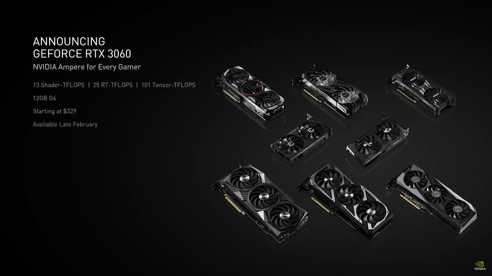
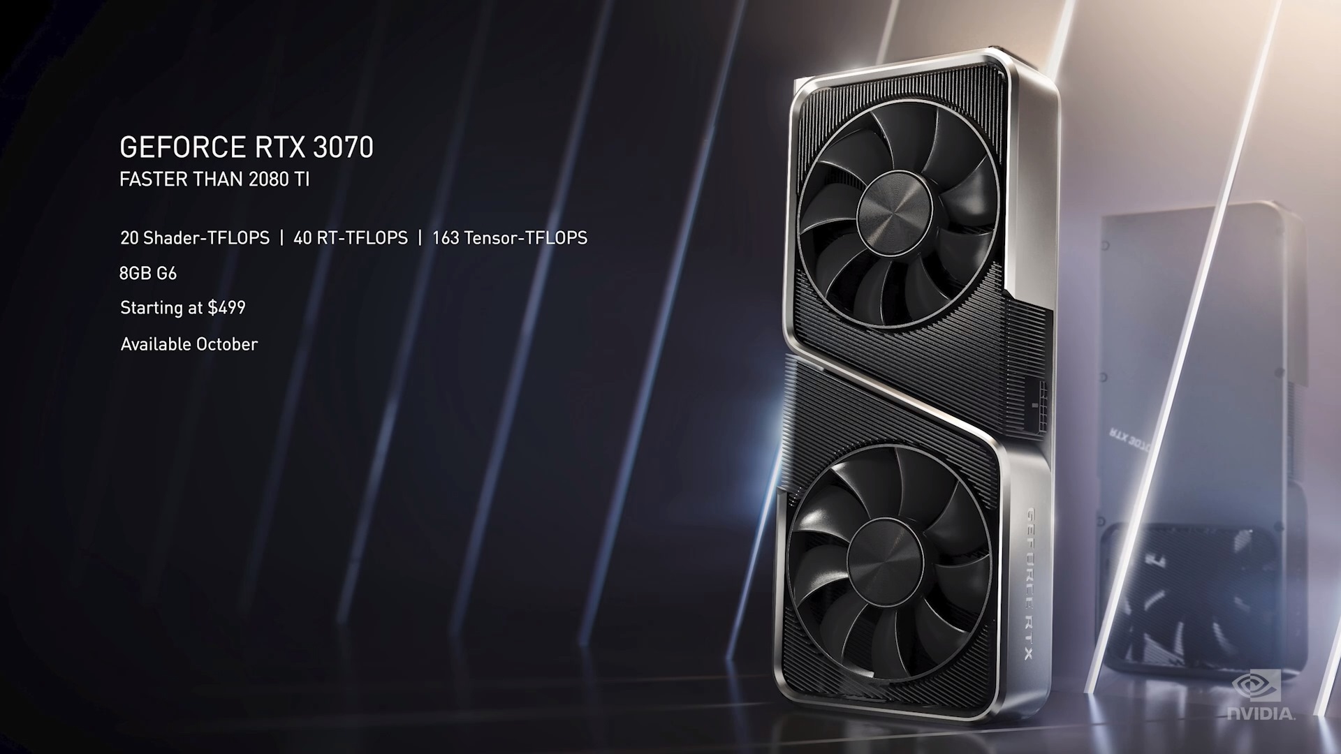
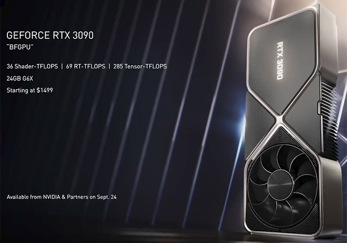
So I think you get the point, well you don’t as I haven’t actually pointed it out . Notice how they all have “RT TFLOPS”?
This in and of itself is interesting, the RT performance seems to be near double the FP32 performance of the cards.
NVidia did a comparison of the “RT TFLOPS” between Turing and Ampere in their white paper:
“A full GA102 GPU incorporates 10752 CUDA Cores, 84 second-generation RT Cores, and 336 third-generation Tensor Cores, and is the most powerful consumer GPU NVIDIA has ever built for graphics processing. A GA102 SM doubles the number of FP32 shader operations that can be executed per clock compared to a Turing SM, resulting in 30 TFLOPS for shader processing in GeForce RTX 3080 (11 TFLOPS in the equivalent Turing GPU). Similarly, RT Cores offer double the throughput for ray/triangle intersection testing, resulting in 58 RT TFLOPS (compared to 34 in Turing). Finally, GA102’s new Tensor Cores can process sparse neural networks at twice the rate of Turing Tensor Cores which do not support sparsity, yielding 238 sparse Tensor TFLOPS in RTX 3080 compared to 89 non-sparse Tensor TFLOPS in RTX 2080.”
What can be gleaned from this information? Drake, if we are to assume to be 3TFLOPs docked, would be close to 6TFLOPs of RT performance.
For cross reference that is ultimately meaningless but just interesting to see (or is it meaningless? ), Andre Goodson of XBox System Architect has claimed that the XBox series X, when leveraging the RT and the shader, would be “over 25TFLOPs” of compute. This comes from the 12TFLOPs of the machine and “over 13TFLOPS” of what the dedicated hardware acceleration would do for RT.

 wccftech.com
we can loosely apply this to the other consoles as well and perhaps to AMD’s GPUs.
Drake? ~6 “RT TFLOPs”
Series S? 5 “RT TFLOPs”?
PS5? 11RT TFLOPs”?
Series X is “over 13 RT TFLOPs”
Note: these are just guesses, could be way off the mark.
Though, I may have figured out how to calculate the individual RT units. each RT core has what I’m just going to call “250 subdivisions” that do twice the work per clock, so, 84*250*2*1860 is close to the 78 “RT FLOPS”
And you can apply it to the others.
You get as close to the actual thing.
And NVidia called the 29.77 TFLOP 3080 a “30 TFLOP” card so it’s probably correct.
20*250*2*1777= 17.77 RT TFLOPs (RTX 3050)
Unsure what to do with this information but post it here.
Edit: AMD’s Ray Accelerators might have “subdivisions of 72” that execute 2 “RT FLOPs” per clock tied with the shaders. So, 52*72*2*1825= 13.665 “RT TFLOPs”
If that makes sense
So, Series S is 4.5 RT TFLOPs maybe? PS5 is 11.5 RT TFLOPs maybe?
AGAIN, these are just theoreticals.
So I think you get the point, well you don’t as I haven’t actually pointed it out
. Notice how they all have “RT TFLOPS”?This in and of itself is interesting, the RT performance seems to be near double the FP32 performance of the cards.
NVidia did a comparison of the “RT TFLOPS” between Turing and Ampere in their white paper:
“A full GA102 GPU incorporates 10752 CUDA Cores, 84 second-generation RT Cores, and 336 third-generation Tensor Cores, and is the most powerful consumer GPU NVIDIA has ever built for graphics processing. A GA102 SM doubles the number of FP32 shader operations that can be executed per clock compared to a Turing SM, resulting in 30 TFLOPS for shader processing in GeForce RTX 3080 (11 TFLOPS in the equivalent Turing GPU). Similarly, RT Cores offer double the throughput for ray/triangle intersection testing, resulting in 58 RT TFLOPS (compared to 34 in Turing). Finally, GA102’s new Tensor Cores can process sparse neural networks at twice the rate of Turing Tensor Cores which do not support sparsity, yielding 238 sparse Tensor TFLOPS in RTX 3080 compared to 89 non-sparse Tensor TFLOPS in RTX 2080.”
What can be gleaned from this information? Drake, if we are to assume to be 3TFLOPs docked, would be close to 6TFLOPs of RT performance.
For cross reference that is ultimately meaningless but just interesting to see (or is it meaningless?
), Andre Goodson of XBox System Architect has claimed that the XBox series X, when leveraging the RT and the shader, would be “over 25TFLOPs” of compute. This comes from the 12TFLOPs of the machine and “over 13TFLOPS” of what the dedicated hardware acceleration would do for RT.
Microsoft: Xbox Series X Performance Is 25+ TFLOPs when Ray Tracing; I/O Rate Equal to 13 Zen 2 Cores
Microsoft's Andrew Goossen said Xbox Series X performance is 25+ TFLOPs when raytracing. The IO rate is equal to a PC with 13 Zen 2 cores.
we can loosely apply this to the other consoles as well and perhaps to AMD’s GPUs.
Drake? ~6 “RT TFLOPs”
Series S? 5 “RT TFLOPs”?
PS5? 11RT TFLOPs”?
Series X is “over 13 RT TFLOPs”
Note: these are just guesses, could be way off the mark.
Though, I may have figured out how to calculate the individual RT units. each RT core has what I’m just going to call “250 subdivisions” that do twice the work per clock, so, 84*250*2*1860 is close to the 78 “RT FLOPS”
And you can apply it to the others.
You get as close to the actual thing.
And NVidia called the 29.77 TFLOP 3080 a “30 TFLOP” card so it’s probably correct.
20*250*2*1777= 17.77 RT TFLOPs (RTX 3050)
Unsure what to do with this information but post it here.
Edit: AMD’s Ray Accelerators might have “subdivisions of 72” that execute 2 “RT FLOPs” per clock tied with the shaders. So, 52*72*2*1825= 13.665 “RT TFLOPs”
If that makes sense
So, Series S is 4.5 RT TFLOPs maybe? PS5 is 11.5 RT TFLOPs maybe?
AGAIN, these are just theoreticals.
Last edited:
OP
OP
There's a possibility that Drake (T239) could use the Cortex-A78C instead of the Cortex-A78AE for the CPU.
According to Arm, the Cortex-A78C allows for up to 8 CPU cores per CPU cluster as opposed to up to 4 CPU cores per CPU cluster for the Cortex-A78AE. This means that the Cortex-A78C requires less clusters for more CPU cores in comparison to the Cortex-A78AE (e.g. 1 CPU cluster for 8 CPU cores for the Cortex-A78C vs 2 CPU clusters for 8 CPU cores for the Cortex-A78AE, 2 CPU clusters for 12 CPU cores for the Cortex-A78C vs 3 CPU clusters for 12 CPU cores for the Cortex-A78AE, 2 CPU clusters for 16 CPU cores for the Cortex-A78C vs 4 CPU clusters for 16 CPU cores for the Cortex-A78AE, etc.). And I imagine more CPU clusters take up more die space.
And the Cortex-A78C happens to allow up to 8 MB of L3 cache vs up to 4 MB of L3 cache for the Cortex-A78AE.
Dakhil, Alovon, 10k and myself go over Drake and the current known information. I think speculation can sometimes move us away from what we actually know, so hopefully this discussion helps frame what this successor is for everyone who watches it.
Just to add to the original post, as @Alovon11 mentioned during the latest NES transmission podcast episode, latency could also be reduced when using the Cortex-A78C vs the Cortex-A78AE, since there are less hardware components Drake needs to communicate with overall when using the Cortex-A78C vs the Cortex-A78AE. In a hypothetical scenario where Nintendo decides to use 8 CPU cores, with the Cortex-A78C, Drake only needs to communicate with 1 CPU cluster since the Cortex-A78C allows up to 8 CPU cores per 1 CPU cluster. However, with the Cortex-A78AE, Drake needs to communicate with 2 CPU clusters individually since the Cortex-A78AE only allow up to 4 CPU cores per 1 CPU cluster. (I say hypothetical since there's no official confirmation Nintendo's using 8 CPU cores. But I do feel like the likelihood of Nintendo using 8 CPU cores for Drake is relatively high.)
(The Exynos 2200 die shot is shown starting at 12:17 in the video.)
So Exynos 2200 has a die size of 99.9 mm² according to a screenshot of a page from the "The Art of Scaling: Distributed and Connected to Sustain the Golden Age of Computation" paper posted on Meeco.
ArchedThunder
Uncle Beerus
- Pronouns
- He/Him
It looks bad on a screen smaller than the Switch’s to me.To be fair, would you actually notice it that much on such a small screen?
Blurry games are eternal
I’d rather we just have clean, stable looking games.The really question is would you prefer Xenoblade Chronicles 2’s worst case scenarios as it is now, or would you prefer to have it use some AI upscaling to achieve a much better result on handheld mode, with a much smoother framerate to boot?
Threadmarks
View all 18 threadmarks
Reader mode
Reader mode
Recent threadmarks
Poll #3: When do you think is the launch window for Nintendo's new hardware? Announcement regarding links to news and rumours from 2022 and 2021 Rough summary of the 2 August 2023 episode of Nate the Hate Rough summary of the 11 September 2023 episode of Nate the Hate Anatole's deep dive into a convolutional autoencoder Differences between T234 and T239 Rough summary of the 19 October 2023 episode of Nate the Hate necrolipe's Twitter (X) post on why a 2025 launch doesn't automatically make T239 outdated based on one of the leaked slides from MicrosoftPlease read this new, consolidated staff post before posting.
Furthermore, according to this follow-up post, all off-topic chat will be moderated.
Furthermore, according to this follow-up post, all off-topic chat will be moderated.
Last edited by a moderator: