Look over there
Bob-omb
Whoever came up with the marketing idea to lump the different features together under the "DLSS 3.x" brand was clearly out of the loop with regards to the upcoming features roadmap.
The Series S as is uses five chips (160-bit bus width). And they're 2 GB each. Unfortunately, 2 GB is as dense as it gets for GDDR6.
Technically, there are two options to increase RAM here. One realistic, the other "Hahaha...no".
The realistic one is to widen the memory bus so you can add more chips.
The 'technically exists' option is something that I think is referred to as clamshell mode? You can actually double the number of chips, but you don't increase bandwidth. I think that it's called clamshell because the usual approach is to put that second set of chips on the other side. It also jacks up the complexity of the PCB design to accommodate those chips on the other side. In the end, it's very rare for this option to actually be used (see the 4060 TI 16 GB version*)
*so, the 4060 TI. 128-bit bus width, so normally four chips. Using 2 GB chips, we get 8 GB total. People weren't too fond of that. Nvidia probably foresaw that, so not too long later, we got a 16 GB version.
For a $100 more. I'd say that's a combination of price of 4 more chips, price of labor in PCB redesign, plus a little extra 'of course we're extracting a premium from you if you're going to turn your nose up at the lower SKUs'.
---
Regarding latency for GDDR6; it's worth noting that ~140ns figure comes from Aida64. For those reading, if you remember I earlier linked to Anandtech and Chipsandcheese for the 12900k, they're not using Aida, so I wouldn't recommending mixing the assorted figures.
 www.tomshardware.com
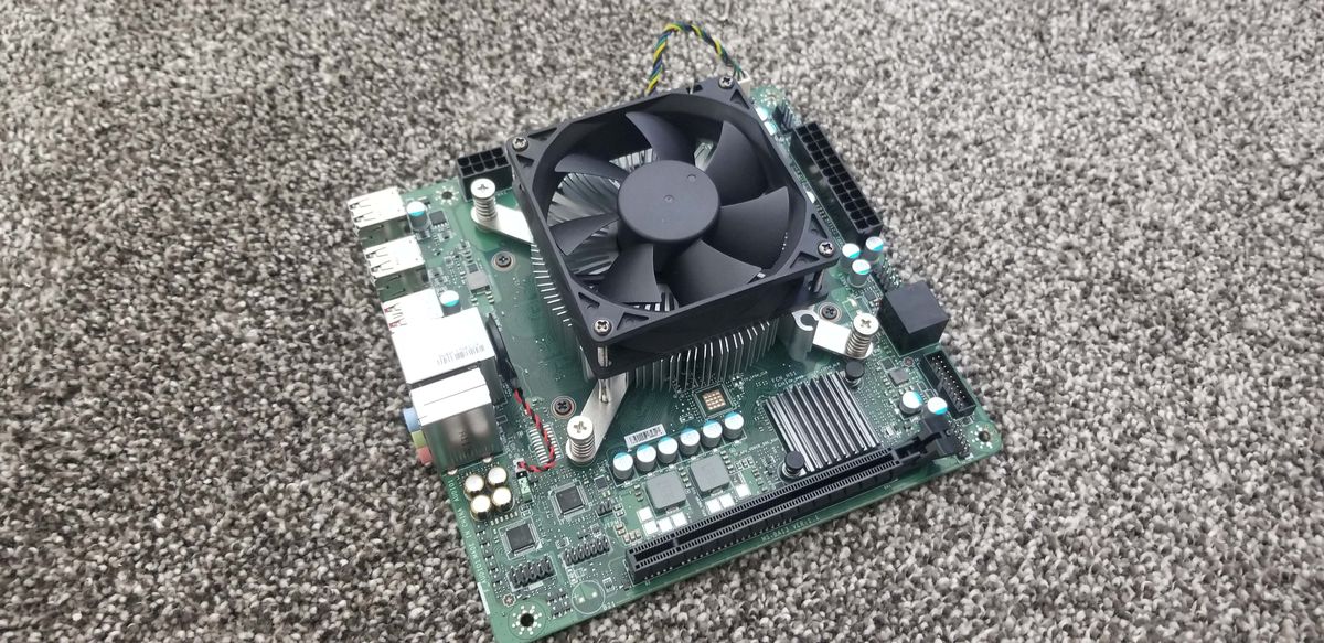
(the 4700S is a PS5 chip with defective iGPU)
www.tomshardware.com
(the 4700S is a PS5 chip with defective iGPU)
The latency chart on this page does include usage of a tool made by someone from Chipsandcheese which tests to a far further depth (up to 1 GB).
I guess it does hang around in the ~140 ns range up to a little further past 64 MB. Then your L3 hit rate keeps tanking until plateauing past 256 MB (at which point you're basically never hitting the 4 MB L3)? The other neat thing to notice is the difference in rate of change between the GDDR6 and DDR4.
So anyway, I think that ~246 ns is more accurate for describing when specifically needing to go out to GDDR6 for the PS5 chip.
Ugh, wish I really understood those benchmark tests more, to be able to truly grok when/how much the difference between the 4750G and 4700S is due to one factor, when/how much is it the other factor. (on paper, the 4750G should clock up to 400 mhz higher, plus is using DDR4-3200 ram for better latency)
Increasing RAM and bus width are, for the most part, tied together.To play devil's advocate, Microsoft could have increased the amount of RAM the Xbox Series S has (e.g. 12 GB GDDR6, with 10 GB reserved for video games, and 2 GB reserved for the OS) and/or increased the RAM bus width (e.g. 256-bit), from the beginning. Alex Battaglia from Digital Foundry has heard from third party developers that the RAM is the Xbox Series S's biggest bottleneck. And besides, Microsoft's already selling the Xbox Series S at a loss.
The Series S as is uses five chips (160-bit bus width). And they're 2 GB each. Unfortunately, 2 GB is as dense as it gets for GDDR6.
Technically, there are two options to increase RAM here. One realistic, the other "Hahaha...no".
The realistic one is to widen the memory bus so you can add more chips.
The 'technically exists' option is something that I think is referred to as clamshell mode? You can actually double the number of chips, but you don't increase bandwidth. I think that it's called clamshell because the usual approach is to put that second set of chips on the other side. It also jacks up the complexity of the PCB design to accommodate those chips on the other side. In the end, it's very rare for this option to actually be used (see the 4060 TI 16 GB version*)
*so, the 4060 TI. 128-bit bus width, so normally four chips. Using 2 GB chips, we get 8 GB total. People weren't too fond of that. Nvidia probably foresaw that, so not too long later, we got a 16 GB version.
For a $100 more. I'd say that's a combination of price of 4 more chips, price of labor in PCB redesign, plus a little extra 'of course we're extracting a premium from you if you're going to turn your nose up at the lower SKUs'.
---
Regarding latency for GDDR6; it's worth noting that ~140ns figure comes from Aida64. For those reading, if you remember I earlier linked to Anandtech and Chipsandcheese for the 12900k, they're not using Aida, so I wouldn't recommending mixing the assorted figures.
AMD 4700S Review: Defective PlayStation 5 Chips Resurrected
Break out the broken chips
The latency chart on this page does include usage of a tool made by someone from Chipsandcheese which tests to a far further depth (up to 1 GB).
I guess it does hang around in the ~140 ns range up to a little further past 64 MB. Then your L3 hit rate keeps tanking until plateauing past 256 MB (at which point you're basically never hitting the 4 MB L3)? The other neat thing to notice is the difference in rate of change between the GDDR6 and DDR4.
So anyway, I think that ~246 ns is more accurate for describing when specifically needing to go out to GDDR6 for the PS5 chip.
Ugh, wish I really understood those benchmark tests more, to be able to truly grok when/how much the difference between the 4750G and 4700S is due to one factor, when/how much is it the other factor. (on paper, the 4750G should clock up to 400 mhz higher, plus is using DDR4-3200 ram for better latency)