
Steve
Chain Chomp
- Pronouns
- he/him
Relax, we'll have ubisoft to the annual fuck up and leak the specs.At the end of the day, nothing we have is gospel. It's all discussion and speculation.
Have faith in me brother.

Relax, we'll have ubisoft to the annual fuck up and leak the specs.At the end of the day, nothing we have is gospel. It's all discussion and speculation.

 viewsync.net
 .
.
Thinking about Switch 3 and BC. Does anyone here have experience with aarch32 and aarch64 and have any concept of emulation overhead to emulate aarch32 on aarch64? I'm only asking this because of old references to some ports having 32bit binaries which works fine on Switch 1 (and presumably Switch 2), but support for aarch32 is being deprecated in newer ARM designs. Google hasn't been terribly helpful for various reasons - some of which may be a lack of skill on my part towards googling the right terms.
Take a look at this:
"
FLAPPY BIRD FLAPS ON!Qualcomm's Snapdragon 8 Gen 3 does not have any CPU cores that support AArch32 (32-bit Arm apps). Despite this, the Xiaomi 14 series is able to run 32-bit Arm apps like Flappy Bird, as shown below by
@realMlgmXyysd
.How is this possible?MlgmXyysd did some digging, and discovered that Xiaomi integrated a 32-bit to 64-bit Arm binary translator called "Tango" from a company called Amanieu Systems. You can find the Tango binaries under /system_ext/bin in the Xiaomi 14's firmware.Their original post (in Chinese) talks a bit more about how this tool is integrated into the build and, more interestingly, how it performs. Links in the reply.
"

 www.amanieusystems.com
www.amanieusystems.com
www.amanieusystems.com
I'm counting on it!Relax, we'll have ubisoft to the annual fuck up and leak the specs.
Have faith in me brother.
The Nvidia leak and literal years of people doing math with its contents to come up with Switch 2's possible spec range is not exactly "hopium."
I mean, doing math to figure out a range of target specs and predicting release timing are two different things?I’m not gonna get into this argument, but this thread is years intelligent, well-meaning hopium-fueled fan-fiction math and theory-crafting:
From
“Team 2020”
“No wait 2021
“Definitely 2022”
“Based on history… 2023”
“Can’t fail 2024”
To
“It can’t be 8nm”
I don’t post here often anymore and this will be my last response for a while.
It’s been mostly fun!
if you can't see the difference in these or basic "learn new info, adjust accordingly", I question if you were even here for honest discussion. you leaving just might be the best thing thenI’m not gonna get into this argument, but this thread is years intelligent, well-meaning hopium-fueled fan-fiction math and theory-crafting:
From
“Team 2020”
“No wait 2021
“Definitely 2022”
“Based on history… 2023”
“Can’t fail 2024”
To
“It can’t be 8nm”
I don’t post here often anymore and this will be my last response for a while.
It’s been mostly fun!
I find it funny and a bit sad that consoles are just becoming into glorified PCs. Like i'm really interested seeing how the console market will look in the next 5-10 since Nintendo will be the only one having that console feel. But maybe i'm just overreacting
Remind me of an Iwata quote
Well... 2020-2022 were mostly switch pro leaks, which Nintendo sadly cancelled because of chip shortage and as well of the switch still selling massively.I’m not gonna get into this argument, but this thread is years intelligent, well-meaning hopium-fueled fan-fiction math and theory-crafting:
From
“Team 2020”
“No wait 2021
“Definitely 2022”
“Based on history… 2023”
“Can’t fail 2024”
To
“It can’t be 8nm”
I don’t post here often anymore and this will be my last response for a while.
It’s been mostly fun!
This has been my thinking lately too. A lot of things that people assumed couldn't be true because it would be bad ending up being true. Could be the same for 8nm.I’m not gonna get into this argument, but this thread is years intelligent, well-meaning hopium-fueled fan-fiction math and theory-crafting:
From
“Team 2020”
“No wait 2021
“Definitely 2022”
“Based on history… 2023”
“Can’t fail 2024”
To
“It can’t be 8nm”
I don’t post here often anymore and this will be my last response for a while.
It’s been mostly fun!
This has been my thinking lately too. A lot of things that people assumed couldn't be true because it would be bad ending up being true. Could be the same for 8nm.
I remember last year when people in this thread kept doubting Nate for thinking that late 2024 was much more likely than late 2023.
Kepler's now saying that the GPU on the PlayStation 5 Pro's APU inherits the Wave Matrix Multiply Accumulate (WMMA) feature from RDNA 4.
Was wondering, i've been hearing a lot of negative of 8NM, what would be the positive? just for a hypothetical if for some reason Nintendo decided to go for it.8nm would just be extremely funny though as we know this system has to be pretty powerful based on the tech demos so this would have to be a just massive device.
Was wondering, i've been hearing a lot of negative of 8NM, what would be the positive? just for a hypothetical if for some reason Nintendo decided to go for it.
Because we know the switch 2 is a 8 inch screen and that's pretty much it.
trying to discredit everything that's been found from the leaks as "fan fiction" by equating it to release timing theories is such a false equivalence that I'm sincerely wondering if you're doing a bitI’m not gonna get into this argument, but this thread is years intelligent, well-meaning hopium-fueled fan-fiction math and theory-crafting:
From
“Team 2020”
“No wait 2021
“Definitely 2022”
“Based on history… 2023”
“Can’t fail 2024”
To
“It can’t be 8nm”
I don’t post here often anymore and this will be my last response for a while.
It’s been mostly fun!
And you'll be leading to error as anything that he said regarding Switch 2 up until now is specluation, or guess or was taken from this exactly thread finds over the last yearsI’ve been following him for a few years and I don’t know of a single leaker who is better than him across gaming or hardware.
No one is perfect but I’ll take his word over any hopium on here.
Edit: typo fixesOk. You don't consider it such.
Others do. That was my entire point.
Your viewport of the world does not see the entire thing all at once, and nobody's can, but you can't make definitive statements about the markets, living environments and tastes of others purely based on your own window.
Size is a factor to LOTS of people, and Nintendo has intentionally marketed the Switch not only as a hybrid, but a home console and a handheld. Because it is one. It is a home console. Nintendo considers it one.
People MAY find a way to make a big console work. But then what's the point, aren't consoles meant to be the easy, don't have to think about it option? That doesn't track. It's just part of how Switch is viewed, used and marketed; its small size is appealing.
This reminds me of one of the biggest praises I've ever seen anyone give a console, it was Yahtzee Croshaw of Zero Punctuation ~ Fully Ramblomatic fame, when he said Nintendo Switch is the only console thst lives in his LIVING ROOM. Because it's small, so it's easy to set up, and has a wide variety of games! He's a notoriously HARSH critic, that is his brand, and one of his biggest compliments he's ever given a console is "easy to set up". A full time video game journalist, an office full of every variation of every relevant bit of hardware he could want. And what wins, at the end of the day? Convenient, easy to transport, easy to set
Wait is this true? We know from information in the leak that the GPU consumes 4.2 watts and runs at 660MHz undocked?from the hack, we know they were testing a portable GPU clock that consumed 4.2w, they didn't test any other clocks, so the assumption for the GPU's power draw should be 4.2w until we have better information, and that clock they tested was 660MHz. We have the answer here
And Kepler's saying that PlayStation 5 Pro's APU inherits RDNA 4's ray tracing technology based on additional PlayStation 5 Pro devkit information.
So I do wonder how close can Nintendo's new hardware can reach the PlayStation 5 Pro in terms of ray tracing with the help of ray reconstruction. (I'm not saying Nintendo's new hardware's going to be on par with the PlayStation 5 Pro in terms of ray tracing.)
I disagree. I think he is an incredibly reliable Intel/Nvidia/AMD leaker.
It's Emily roger all over again (the prolific NX leaker)Okay? Even if that’s true (I’m skeptical), doesn’t mean he’s a reliable Nintendo leaker.

wafers are cheaper, but you're also getting less product per chipWas wondering, i've been hearing a lot of negative of 8NM, what would be the positive? just for a hypothetical if for some reason Nintendo decided to go for it.
Because we know the switch 2 is a 8 inch screen and that's pretty much it.
It would be very cheap and thus we would be able to have a cheaper Switch 2 (Or Nintendo would have better margins at launch) or Nintendo could use the savings from the SoC manufacturing and spend them elsewhere (new gimmick, better screen, bigger battery, more RAM, etc).Was wondering, i've been hearing a lot of negative of 8NM, what would be the positive? just for a hypothetical if for some reason Nintendo decided to go for it.
Because we know the switch 2 is a 8 inch screen and that's pretty much it.
Except 8nm isn't cheaper. Per wafer is cheaper, but you get lesser (poorer yields and lower density).It would be very cheap and thus we would be able to have a cheaper Switch 2 (Or Nintendo would have better margins at launch) or Nintendo could use the savings from the SoC manufacturing and spend them elsewhere (new gimmick, better screen, bigger battery, more RAM, etc).
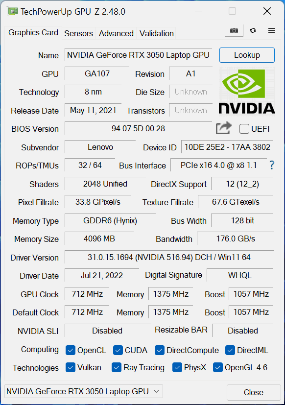
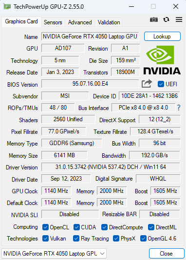
I was watching a DaveDoesStuff video about the RTX 2050 and one of the things that catched my eye was this:I was looking at some benchmark recently and saw that laptopmedia had covered quite a few benchmark/gameplay footages with various laptop GPUs (e.g. RTX 2050 @ 35W, RTX 3050 @ 65W-75W, RTX 4050 @ 45W).
Now, of course, there's some variance with the results due to the CPU being used and perhaps even memory clock speed having an impact. I checked most of the benchmarks and the laptops or spec's they use and I'd say they're relatively close in capabilities. Although the amount of metrics on display isn't giving much validity, I know they're a legit source. One note to make is that they may not have been made with the same drivers....
Nonetheless, perhaps for a layman's showcase of how node process/power efficiency/clock speed all play a role.
I put a side-by-side of Death Stranding, and it's quite impressive how the RTX 4050 performs, practically doubles compared to the RTX 2050, with only a 10W increase of TGP, while also leading the RTX 3050 that has a 20W higher power consumption. Now there could be dynamic boost being at play (and other variables), although I suspect these laptops are hitting their max-rated TGP; 35W, 65W, 45W for the RTX 2050, 3050, 4050 respectively.
ViewSync - Multiple YouTube Viewer
Streamlined multiple YouTube viewer with built-in support for content creators.
I guess ideally, you’d want to compare at the same clock frequency and then observe the power consumption - frametime, but for such an analysis you’d need to have each of these devices (and a vbios that allows to have similar ranges of frequencies). Also the RTX 4050 has more CUDA cores (2056), maybe the RTX 500 (2048 CUDA cores) can give some interesting metrics. but given the recent announcement of that chip, it’ll take a while
RTX 2050 [35W]
As per TPU; GeForce RTX 2050 35W = 982-1372 MHz
RTX 3050 [65W]
RTX 4050 [45W]


If you only pay for the working chips, yields barely matter. About yields, Samsung 8nm is a mature node with high yields at this point. They struggled with initial Ampere GPUs per rumors, but over time everything was resolved. The only point of comparison between SEC 8N and TSMC 4N that we had was SemiAnalysis claim that 4N had slightly better parametric yields while having the same catastrophic yields as 8N.Except 8nm isn't cheaper. Per wafer is cheaper, but you get lesser (poorer yields and lower density).
Yeah - my view is that both 4N and SEC8N are the most likely candidates, with 4N being more likely if 12SMs claim is still true.If you only pay for the working chips, yields barely matter. About yields, Samsung 8nm is a mature node with high yields at this point. They struggled with initial Ampere GPUs per rumors, but over time everything was resolved. The only point of comparison between SEC 8N and TSMC 4N that we had was SemiAnalysis claim that 4N had slightly better parametric yields while having the same catastrophic yields as 8N.
Density, yes. But T239 would still be a small chip due to having a small GPU. GA107 (20 SMs) is around 19x mm² die size on 8N.
Granted, I personally expect TSMC 4N. But I believe 8N might be possible on a 10W budget for portable.
So you're telling me MLID making claims about Nintendo switching back to AMD is credible?I’ve been following him for a few years and I don’t know of a single leaker who is better than him across gaming or hardware.
No one is perfect but I’ll take his word over any hopium on here.
Not if Sony makes it a time exclusive.if SE is going to bring KH4 to Drake, then I expect the KH Collection to get native ports. cloud isn't serving anyone at the moment
Funny thing, I was telling someone that earlier today.If we can get 1080p>4K, path tracing on high detail virtualized geometry next gen, that would be good enough to stop on. No need for PS7 etc.
The problem is that 12 SM isn't a "claim", it was datamined directly from Nvidia's servers, and given that it was from a graphics API, there were no redundant SMs like with the PS5 and XSX GPUs. A 12 SM T239 is just the indisputable reality, and any speculation on node has to be made with that information in mind, otherwise it's completely meaningless.Yeah - my view is that both 4N and SEC8N are the most likely candidates, with 4N being more likely if 12SMs claim is still true.
Just sharing that I'm not sure SEC8N is cheaper compared to TSMC 4N when considering how many chips one can get from those node processes.
Hidden content is only available for registered users. Sharing it outside of Famiboards is subject to moderation.
Pretty much. To be honest, I'm kinda past the node talk. I know Nintendo will deliver a device with reasonable battery life and weight. And we also know it can run the Matrix Awakens demo and BoTW at 4K60 (DLSS). So the node is basically academic at this point. Whichever it is, Nintendo will be able to get their performance, area and energy objectives from it.I agree it's small chip either way (fitting inside that substrate space). Mostly a matter of power draw concerns if we're still looking at 12SMs.
MLID pretty much said that he believes that the Switch in portable mode will be around stream deck and below the Series S in dock mode.... the same thing everyone concluded around here.I disagree. I think he is an incredibly reliable Intel/Nvidia/AMD leaker.
I think it is ok for anyone here to say they don't understand the technical discussion here. While I understand stuff like ray tracing, the BVH, and other software related stuff sure I can hang. When it comes to power draw and the lithographic process, I don't understand.The Nvidia leak and literal years of people doing math with its contents to come up with Switch 2's possible spec range is not exactly "hopium."
Hey man, if we're able to boost most of Nintendo first party games at 4k 60fps (DLSS), that would be hella nice and i can personality see it being part of the marketing. Like the switch library is probably one of Nintendo best and people are still paying full price for these games.Pretty much. To be honest, I'm kinda past the node talk. I know Nintendo will deliver a device with reasonable battery life and weight. And we also know it can run the Matrix Awakens demo and BoTW at 4K60 (DLSS). So the node is basically academic at this point. Whichever it is, Nintendo will be able to get their performance, area and energy objectives from it.

MLID is saying that Switch 2 is 3 to 4 TFLOPs, just like us. being hung up on 8nm, is a fools erran, it literally doesn't matter what size the transistors are, they only tell us the possible performance, which we've pegged at 3 to 4 TFLOPs for years. MLID didn't disprove anything in this thread, he is saying it can be done on 8nm, which I personally think is stupid, but it doesn't conflict with my performance expectations at all.I’m not gonna get into this argument, but this thread is years intelligent, well-meaning hopium-fueled fan-fiction math and theory-crafting:
From
“Team 2020”
“No wait 2021
“Definitely 2022”
“Based on history… 2023”
“Can’t fail 2024”
To
“It can’t be 8nm”
I don’t post here often anymore and this will be my last response for a while.
It’s been mostly fun!
Yeah, the DLSS test was done with that clock and the clock's test was named "4.2w" Drake didn't exist for another ~9 months though, so these are just targets.Wait is this true? We know from information in the leak that the GPU consumes 4.2 watts and runs at 660MHz undocked?
For years my thought on Dragon Quest XII is Switch 2 is no question, the only question is whether they're confident enough to skip Switch 1. With the exception of V being a relatively early SNES game, Dragon Quest has really only arrived on mature platforms with high userbase (plus things like PS4 or MSX adding on), even if that machine's successor is already out. Something like a PS5+Switch 2 release in 2025 or 2026 might have limited sales potential (in Japan) versus VIII launching to a userbase of 15 million, let alone compared to IX launching to a userbase of 30 million, or XI launching to userbases of 23+5 million.I would guess Dragon Quest XII and Kingdom Hearts 3 will be on Switch 2 ... KH3 is on Switch already just is cloud streaming. DQXI was on Switch so DQXII would make sense, Enix won't ignore the no.1 selling platform in Japan.
Positive: More room for improvement in the future when they decide to go Not 8nm.Was wondering, i've been hearing a lot of negative of 8NM, what would be the positive? just for a hypothetical if for some reason Nintendo decided to go for it.
Because we know the switch 2 is a 8 inch screen and that's pretty much it.
I think that's referring to some data about DLSS tests that were in the hack. They're without much context, but it's easy to speculate that the specific things tested weren't totally arbitrary.Wait is this true? We know from information in the leak that the GPU consumes 4.2 watts and runs at 660MHz undocked?
All the Sega stuff was Midori, a banned source was Sea of Thieves and Hi-Fi Rush, Necro was Monster Hunter, a Nintendo employee who helps with third party relations was in the credits for BG3 and I'm the source for Red Dead
No idea where Spyro and Crash came from, same with Ridge Racer
That is against both MLID and this thread. MLID is saying the same performance we are. 3TFLOPs to 4TFLOPs. He just thinks Nvidia broke physics.I prefer to expect SEC 8nm with Switch 1 clocks, that way I can't be disappointed (I think lol)
* Hidden text: cannot be quoted. *
No one cares what the node is. You just aren't understanding. The point of discussing the node is to try and figure out the performance of Switch 2, it would limit possible clocks and thus TFLOPs. MLID and this thread agree that the TFLOPs performance range is 3TFLOPs to 4TFLOPs (The DLSS test has a 4.24TFLOPs max clock that is in the leak). There is no conflict here. The debate about process node is to be had by people who do not understand that it is meaningless.So what other information besides Nvidia's leaked data is there to prove it's not 8nm
I was watching a DaveDoesStuff video about the RTX 2050 and one of the things that catched my eye was this:
Which aren't nearly as bad for a 16 SM 8nm GPU at low clocks. Granted, we can't take the software reporting of the TDP at face value as we don't know what the hardware is actually informing, we don't know which parts of the hardware are active or not, etc. But such TDP and clock numbers on 8nm would be quite applicable for an even smaller GPU like GA10F/T239.
If you only pay for the working chips, yields barely matter. About yields, Samsung 8nm is a mature node with high yields at this point. They struggled with initial Ampere GPUs per rumors, but over time everything was resolved. The only point of comparison between SEC 8N and TSMC 4N that we had was SemiAnalysis claim that 4N had slightly better parametric yields while having the same catastrophic yields as 8N.
Density, yes. But T239 would still be a small chip due to having a small GPU. GA107 (20 SMs) is around 19x mm² die size on 8N.
Granted, I personally expect TSMC 4N. But I believe 8N might be possible on a 10W budget for portable.
Pretty much. To be honest, I'm kinda past the node talk. I know Nintendo will deliver a device with reasonable battery life and weight. And we also know it can run the Matrix Awakens demo and BoTW at 4K60 (DLSS). So the node is basically academic at this point. Whichever it is, Nintendo will be able to get their performance, area and energy objectives from it.
Nvidia has pre-paid for so much fabrication at TSMC 4nm capacity that rumors are they have halted production to try and clear stock in order to have demand for the 50 series cards that are expected to come out later this year. My belief for one of the better reasons to put T239 on 4nm, is Nvidia are killing their premium value in the market by over saturating production. I believe on the new 50 series cards they might roll out everything much slower then they did with Lovelace.I think Nvidia has much more incentive to use TSMC's 4N process node to fabricate T239 than Nintendo does, because considering that I imagine Nintendo has exclusivity towards the highest binned T239s to begin with, I think Nvidia wants to avoid a situation of having a surplus of lower binned T239s. And I think Nvidia's going to have a much higher surplus of lower binned T239s with Samsung's 8N process node vs TSMC's 4N process node.
MLID is saying that Switch 2 is 3 to 4 TFLOPs, just like us. being hung up on 8nm, is a fools erran, it literally doesn't matter what size the transistors are, they only tell us the possible performance, which we've pegged at 3 to 4 TFLOPs for years. MLID didn't disprove anything in this thread, he is saying it can be done on 8nm, which I personally think is stupid, but it doesn't conflict with my performance expectations at all.
Yeah, the DLSS test was done with that clock and the clock's test was named "4.2w" Drake didn't exist for another ~9 months though, so these are just targets.
