The lack of camera support rules out being used for self-driving cars, correct? But what about for infotainment units on cars for navigation, games, car play, etc?
In theory they could use it for infotainment, but it's worth noting that Nvidia's infotainment solution (DRIVE IX) advertises
driver safety monitoring (via internal cameras) as one of its key features. I would also imagine that if they were developing it as a cheaper alternative to Orin primarily for infotainment use-cases, they would still leave the door open to ADAS (something TX1 has been used for), as I assume you would still need to pass the same safety certification either way.
To go back to the post to which you are replying--the information in the Linux commits implies that this SoC physically existed in mid-2022, and the SoC existing in mid-2022 implies, based on typical manufacturing timelines, that a device using the SoC would launch sometime in 2023. Is that correct?
If so, and assuming that Nintendo truly is the only consumer of this SoC, is there any way to reconcile the SoC existing in mid-2022 with the only device using it launching in 2024 or 2025?
If Nintendo is the only customer for T239, and it existed in silicon in 2022, but Nintendo won't release anything until 2024, then the only conclusion I could think of is that Nintendo delayed or cancelled their device after T239 had already taped out and hit early manufacturing. That's something that would have seemed very unlikely to me before, but it's technically possible. If the decision was unilateral from Nintendo (ie the chip was good to go but Nintendo just decided not to go ahead) then it would be a very expensive decision, as they'd either have to sit on manufactured chips for a couple of years or presumably pay Nvidia some penalty for pulling out of their contract.
On the other hand, it could have been something outside of Nintendo's control, like the chip not meeting agreed-upon requirements. I've said before that I don't think there's any reasonable possibility that they could have manufactured it on Samsung 8nm and been surprised that a 12 SM GPU would be too power hungry when it came out of manufacturing. I also don't think they would have been surprised by TSMC 7nm/6nm, or TSMC's 5nm/4nm processes. However if they had planned to manufacture on one of Samsung's 5nm or 4nm processes, then they could well have been surprised by how power hungry it ended up being. We know that Qualcomm were so unhappy with Samsung's 4LPE for the Snapdragon 8 Gen 1 that they migrated the entire chip over to TSMC N4 (probably at great expense, given the short timescale). We also know that Samsung themselves had to significantly reduce clocks on the Exynos 2200 GPU to get it out the door.
Conceivably they could have planned to manufacture on a Samsung 5nm or 4nm process, presumably expecting much better performance and power efficiency when they started in 2019/2020 than what they got after tapeout in 2022. I've heard that Nvidia's contract with Samsung has them paying for yielded die rather than per wafer (sorry, can't find the source for that at the moment), and depending on how that contract is written, if none of the dies meet Nvidia and Nintendo's yield criteria, Nvidia wouldn't have to pay Samsung anything. Or, Samsung would be in a position where they have to pump out a huge number of expensive to manufacture dies at a very low yield rate to hit Nvidia's requirements, and they'd be happier to renegotiate their way out of the contract rather than operate at a loss.
In theory we could have a situation where T239 was designed for Samsung 4LPE (let's say), and after taping out in early 2022, early silicon was way behind expectations in power/perf. With Nvidia having an advantageous contract with Samsung, and Nintendo seeing the Switch still selling well, they decide to push back to 2024, on either Samsung 3GAP (which will ship in 2024, with Nvidia rumoured to be one of the customers) or TSMC 4N. Nvidia might even decide to continue with small-scale manufacturing on 4LPE, as their other use-cases (eg Shield TV) don't have such strict yield requirements.
My main issue with this theory is that Nvidia have nothing else being manufactured on any Samsung 5nm or 4nm process. Generally they would want to share manufacturing processes across many product lines, both for economies of scale and to maximise flexibility, so manufacturing a single chip on Samsung 5nm or 4nm while you're planning to manufacture almost everything else on TSMC 4N would have been a pretty strange decision.
I don't think it's out of the question that Nvidia might want to run Linux on the chip entirely for internal development and/or continuous integration purposes.
Yeah, I wouldn't rule that out, but in that case I wouldn't expect to see any T239 code upstreamed to the Linux kernel. Perhaps the upstreamed references are only there incidentally, to ensure that T234 behaviour is consistent between mainline Linux and their internal branches which also support T239, but there have been a few of them now, and it wouldn't be difficult to do so in a way which avoids any T239 references being upstreamed at all.
For the same reason it’s not well-suited for gaming, A78AE CPUs are not well-suited for general purpose consumer computing.
Unlike most other micro PCs, because Nvidia is the SoC maker, they have a better cost for assembly (paying cost instead of wholesale price for a chip and able to leverage binning of an existing product for another customer). For example: Jetson Nano (which Tom’s Hardware called the Raspberry Pi of AI) was sold at some sort of a profit for $99 in 2019. Meanwhile, a 2-core Celeron N3350 micro-PC with 4GB LPDDR3 RAM from Bee-Link will run you $119.
I think Nvidia has an opportunity to basically scoop up nearly all of binned Drake chips and compete with a far more capable SoC in the “cheap office micro PC” market at the VERY least, now that ARM Windows is a LOT better than it was when it started.
It’s not even an unprecedented occurrence,
AMD used binned PS console chips similarly (and priced themselves out of a lot of customers at $400 a pop, methinks).
One of the big issues with T239 being used in a (Windows) PC is that Windows on ARM is currently exclusive to Qualcomm chips. Microsoft would have to be talked out of that exclusivity, and I don't think T239 offers much that they can't get from Qualcomm.
The real advantage T239 (or any Nvidia SoC) would have in the PC space is a capable integrated GPU, but without games being compiled natively for ARM you're still going to end up with pretty poor gaming performance. Perhaps if Nvidia is planning to move into desktop ARM CPUs after Grace, they could use T239 to get their foot in the door, and work with developers to get games ported over to ARM before they launch a desktop lineup.
Project Indy is the Nintendo Switch. Project Indy went through several iterations before landing on what we got, and the name "Nintendo Switch" was given to a product that didn't yet have the TX1 inside it.
There isn't enough data in the gigaleak to say what the hell was going on there, and how that device evolved (and I have my own theories) but here is what is clear.
In the beginning of 2014, Nintendo was building Indy around a custom SOC from ST called Mont Blank. Mont Blanc has two years of development, a custom GPU, and a complete spec sheet with pin outs (though this doesn't mean final hardware).
Mont Blanc was a hybrid 3DS WiiU sorta deal, running 4 ARM cores, but a "decaf" version of the GPU in the WiiU. We can't be certain, but the design seems unlikely to have been as powerful as the Wii U, and so at least at the start of SOC development, the idea was still for a device that would continue the handheld line independently of the TV line.
By August of 2014, this device was called Nintendo Switch. By the end of 2014, the "New Switch" had replaced Mont Blanc with a TX1.
I do not believe there is any document in the gigaleak that indicates when this transition happened, but those who have reviewed it say that Nintendo's discussions do influence TX1's design (IIRC it's security concerns, not performance)
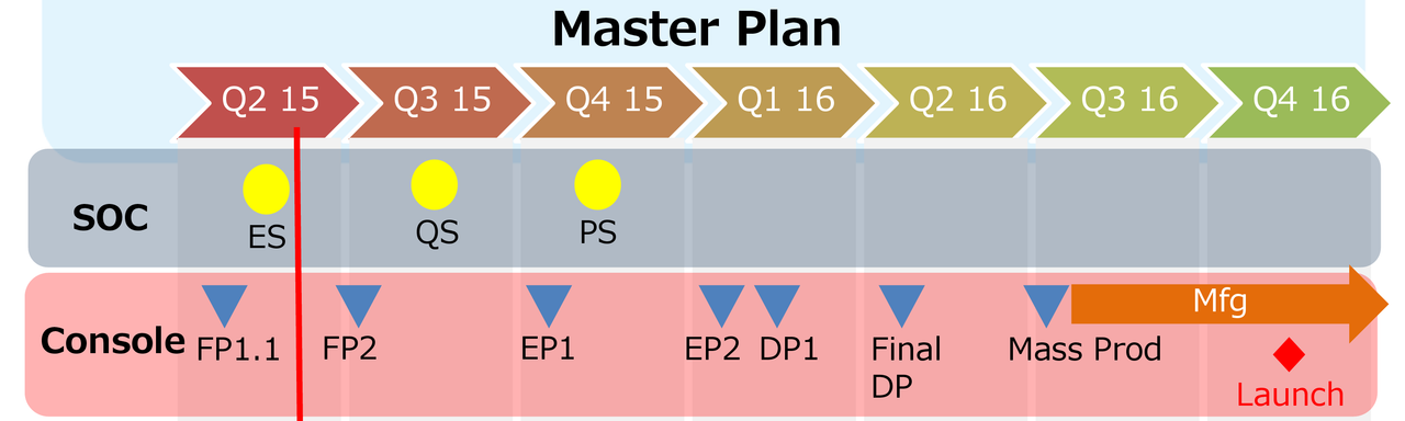
Sometime in Q1 2015, Nintendo builds functional prototype 1 for the Switch, in March, Iwata says the NX is coming during the DeNA press conference, and by June, they're planning to launch in holiday 2016.
So, yes, Nintendo had moved to a TX1 based design before the TX1 launched.
Yes, Nintendo can scrap an SOC with 2 years of custom development.
No, it's unlikely that the SOC manufacturer is going to put your custom chip in rando hardware when you do - Mont Blanc never showed up anywhere.
Some version of the Switch was being developed for 5 years before launch, and yes, some of the hardware designed in that first year wound up in the final product (the DRM hardware on the cartridge reader in the switch was designed in 2012 as part of Indy).
From Pivot to Final Hardware took anywhere from 2 years to 2.5 depending on how you look at it. So yeah, the idea that a device scrapped in mid-2022 would get a replacement out the door in 2024 is precedented.
Again, I'm trying to dodge the narrative a bit here. I suspect that the none of the puzzles pieces seem to fit because not only do we not have all the puzzle pieces, we also don't now what the box looks like.
I haven't read super deep into this, but my understanding is that, although Nintendo chose TX1 before it was manufactured, and may have had some influence in its design, it was already well along the road by that point, and would have launched, and probably looked very similar, regardless of whether Nintendo signed up or not.
My point here is that, while TX1 wasn't
strictly an off-the-shelf chip for the Switch, it might as well have been. It was a chip that was already well in development and would be manufactured well ahead of the planned launch of the Switch, and this allowed them to be so aggressive with their timescale for pushing the Switch out the door. I don't think there's a similar option available to them today.
If they were to drop BC, they could probably get an SoC from Qualcomm or elsewhere that would suit their purposes at short notice, but presumably BC is much more important to them now than it was post-Wii U, which means a chip from Nvidia. In which case, for Nintendo to execute a similar two-year turnaround for the new model, there would need to be a suitable chip already in development at Nvidia. That seems very unlikely to me.
Post-Switch, Nvidia have released only one SoC suitable for consumer devices, TX2 (Parker), which was already in development
long before Nintendo signed up to use the TX1. Since signing Nintendo, the only SoCs Nvidia have announced are Xavier, Orin and Atlan/Thor, all large automotive SoCs unsuitable for consumer devices. As far as we're aware, the only SoC they've made since signing Nintendo that would be suitable for a device like the Switch is T239, which looks very much like it was designed specifically for Nintendo. It would be very surprising to me if they just so happened to have another consumer SoC waiting in the wings for a 2024 release that Nintendo hadn't been involved in at all.


famiboards.com

