So have we heard or discussed this feature yet possibly being included?
It was definitely present in A100 GPU but I wonder if this will make its way over to Drake also...
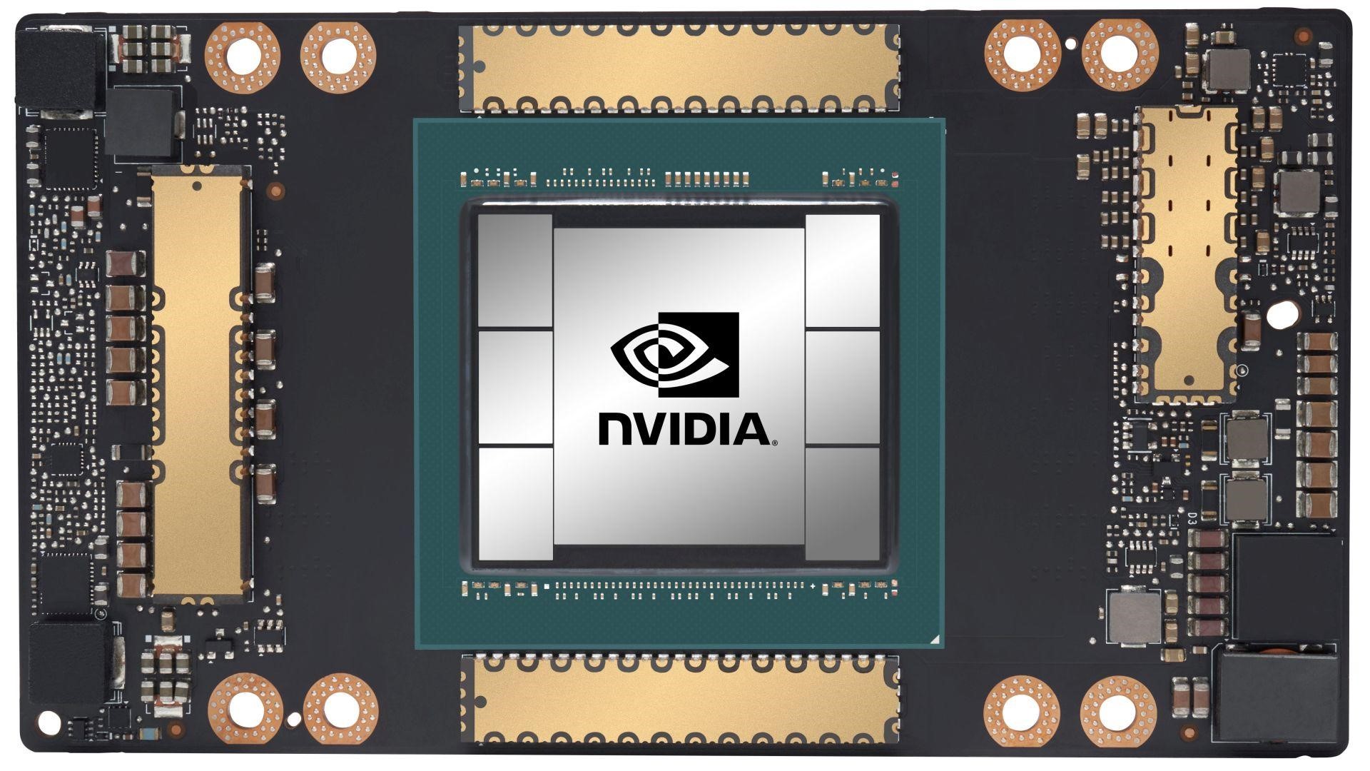
"The NVIDIA Ampere architecture adds Compute Data Compression to accelerate unstructured sparsity and other compressible data patterns. Compression in L2 provides up to 4x improvement to DRAM read/write bandwidth, up to 4x improvement in L2 read bandwidth, and up to 2x improvement in L2 capacity."
Today, during the 2020 NVIDIA GTC keynote address, NVIDIA founder and CEO Jensen Huang introduced the new NVIDIA A100 GPU based on the new NVIDIA Ampere GPU architecture. This post gives you a look…

developer.nvidia.com

Likely patch. It's not like DLSS needs an overhaul in an engine to get it working correctly, though I do wish more developers/publishers tune for a proper balance of IQ/performance.
There does need to be an overhaul though, not a total or complete overhaul but it’s not like a drag and drop thing.
What if everyone is wrong and this isn’t a new Switch but rather a portable Wii U :shock:
The switch in portable mode is like the Wii U docked

Also regarding CPU cores, do you think 8 cores is now far more likely? We have plenty of examples of Samsung 5nm smart phones with octocore setups (writing this on a galaxy s21 with such a setup) and whilst I appreciate phones run in burst, 8 A78s at 1ghz should be doable on such an advanced node.
If it’s on the 5nm node, then it can run at 2-1.9-2.4GHz range not the 1GHz range, at 1GHz it might be
wasting battery life actually.
This would be an enormous leap over the CPU in the current switch, exciting if true. I wonder how close an 8 Core A78C setup at 2GHZ would get to the 8 Core 3.5GHZ setup in the ps5? Are we now talking somewhere around 50% of the power?
It would be around A14 Bionic range. I think.
We don't know about RAM or clocks but it appears the core count (1536) and cache size (2MB I think?) for Drake is higher than both of those.
It’s 4MB!
Which is a lot.
It’s like it’s own mini infinity cache system (which is just more L3$ rebranded for marketing)!
And 1.5-2.3MB of L1$
Personally, I'm not sure that a change in process node would cause a change in codename (while also not changing the name T239). The chip in the original Switch is only known as T210 or GM20B, with the distinction between Erista and Mariko seemingly not present in the leak at all, along with most other information on the "Nintendo side" of things.
I wonder if the code name change has to do with the CPU cores being turned off. Maybe with Erista they (A53) were just turned off, but with Mariko they were just outright disabled aka fused off plus the die shrink.
T210 has them, but T214 doesn’t have them at all.
Just a theory!
They could do like last time they wanted to pretend they weren't releasing a successor to a strong performer and call it a third pillar.
Or like the last time they pretended it was a new generation and it was, internally spec-wise, just a GameCube pro

.
Nintendo has options on what they can do with this. Though as for the other convos going on about it, a platform can have a next generation device without having a clean break of the platform.
A revision that plays less games than base Switch is the most worthless concept for a console I've ever heard.
Right, like it’s the thing that doesn’t make sense to me. A revision is, in essence, the base device so it does what the base device does. If it’s a revision but it can’t do what the base device does, that’s not a revision, it’s just a copy of the original. A fraud (ok harsh) in all accounts.
It would be the switch in
concept only.
The funny thing is that pre leak, this thread has been tsuw (wust backwards).
The constant drive-by’s in this thread, the last thread and the thread before that, the drive by posts in other threads related to the subject, really gaslit us into believing the absolute worst, huh?

Hell, we had a few about if they would even utilize DLSS!