Steve
Koopa
- Pronouns
- he/him
We are so back NintendobrosWake up TSMC 4N believers! Nintendo can now use TSMC 4N because it's an outdated node now


(also is that from the current Nvidia livestream)

We are so back NintendobrosWake up TSMC 4N believers! Nintendo can now use TSMC 4N because it's an outdated node now
Interestingly, Blackwell has a decompression engine. Developed at the same time as Drake's or were they developed separately?

Wake up TSMC 4N believers! Nintendo can now use TSMC 4N because it's an outdated node now
Edit: For context, next-gen DCAI parts from Nvidia are using TSMC 4NP, an evolution of 4N. Probably a further customized 4N with N4P enhancements.
Is that a hint?


From what i understand, nope, this only give us a hint of possible technology for future proyects of Nvidia but nothing elseSo... did the Nvidia presentation tell us something, even maybe a slight hint because the only thing of value would maybe be this.
Was that a confirmation, or was it not the case before?
I see wikipedia articles still saying Lovelace for DRIVE Thor.Was that a confirmation, or was it not the case before?
Was that a confirmation, or was it not the case before?

 nvidianews.nvidia.com
The next-generation superchip comes packed with the cutting-edge AI capabilities first introduced in the NVIDIA Hopper™ Multi-Instance GPU architecture, along with the NVIDIA Grace™ CPU and NVIDIA Ada Lovelace GPU.
 nvidianews.nvidia.com
This next-generation AV platform will integrate the new NVIDIA Blackwell architecture, designed for transformer, LLM and generative AI workloads, which was announced during NVIDIA founder and CEO Jensen Huang's keynote at GTC.
More seriously, something I wanted to know - do "refinement nodes" of this kind that are essentially still just improved versions of the primary node (in this case TSMC 5nm) actually cost more money and see separate pricing for N5, N4, 4N, N4P, 4NP and N4X? Or are they just "this is what 5nm customers get now, for the same money per wafer"?
NVIDIA Flagship Accelerator Specification Comparison | |||
B200 | H100 | A100 (80GB) | |
| FP32 CUDA Cores | A Whole Lot | 16896 | 6912 |
| Tensor Cores | As Many As Possible | 528 | 432 |
| Boost Clock | To The Moon | 1.98GHz | 1.41GHz |
| Memory Clock | 8Gbps HBM3E | 5.23Gbps HBM3 | 3.2Gbps HBM2e |
| Memory Bus Width | 2x 4096-bit | 5120-bit | 5120-bit |
| Memory Bandwidth | 8TB/sec | 3.35TB/sec | 2TB/sec |
| VRAM | 192GB (2x 96GB) | 80GB | 80GB |
| FP32 Vector | ? TFLOPS | 67 TFLOPS | 19.5 TFLOPS |
| FP64 Vector | ? TFLOPS | 34 TFLOPS | 9.7 TFLOPS (1/2 FP32 rate) |
| FP4 Tensor | 9 PFLOPS | N/A | N/A |
| INT8/FP8 Tensor | 4500 T(FL)OPS | 1980 TOPS | 624 TOPS |
| FP16 Tensor | 2250 TFLOPS | 990 TFLOPS | 312 TFLOPS |
| TF32 Tensor | 1100 TFLOPS | 495 TFLOPS | 156 TFLOPS |
| FP64 Tensor | 40 TFLOPS | 67 TFLOPS | 19.5 TFLOPS |
| Interconnect | NVLink 5 ? Links (1800GB/sec) | NVLink 4 18 Links (900GB/sec) | NVLink 3 12 Links (600GB/sec) |
| GPU | "Blackwell GPU" | GH100 (814mm2) | GA100 (826mm2) |
| Transistor Count | 208B (2x10⁴B) | 80B | 54.2B |
| TDP | 1000W | 700W | 400W |
| Manufacturing Process | TSMC 4NP | TSMC 4N | TSMC 7N |
| Interface | SXM | SXM5 | SXM4 |
| Architecture | Blackwell | Hopper | Ampere |
Mario games never have that much bloatdespite Switch sucessor been substancially more powerful then Nintendo Switch, should we expect a significant jump on file size? Super Mario Odyssey for example is 5.6GB, and next 3D Mario is 50GB, can we expect this significant jump? Super Mario Odyssey 5.6GB to next 3D Mario: 8.8GB?
Aren't those tflops weak? 3.6 fp8 means only 0.9 fp32.Wake up TSMC 4N believers! Nintendo can now use TSMC 4N because it's an outdated node now
Edit: For context, next-gen DCAI parts from Nvidia are using TSMC 4NP, an evolution of 4N. Probably a further customized 4N with N4P enhancements.

Aren't those tflops weak? 3.6 fp8 means only 0.9 fp32.
Unless I'm misunderstanding something? I wonder why that number with no mention of clocks. Is that max? I'm all over the place now
Assuming the rest of the Blackwell platform is on 4NP, do we think they're just gonna keep with it for the 50-series? Ampere datacenter chips were a node ahead of the 30-series, and Hopper was the same node as the 40-series, so maybe they don't see 3 nm as worth it and are just waiting for TSMC to switch to GAAFET for N2 and use that for Blackwell-Next?
It should be stressed that Nintendo is also very good with File Size in comparison to other companies. I have little doubt in my mind that they decided to further improve their compression tools to compensate. They might whittle that increase in file size to 3.5, 3 or even twice the size of the games previously if they can get them right.
They're always going to increase whether we like it or not, but Nintendo will likely try to mitigate it.
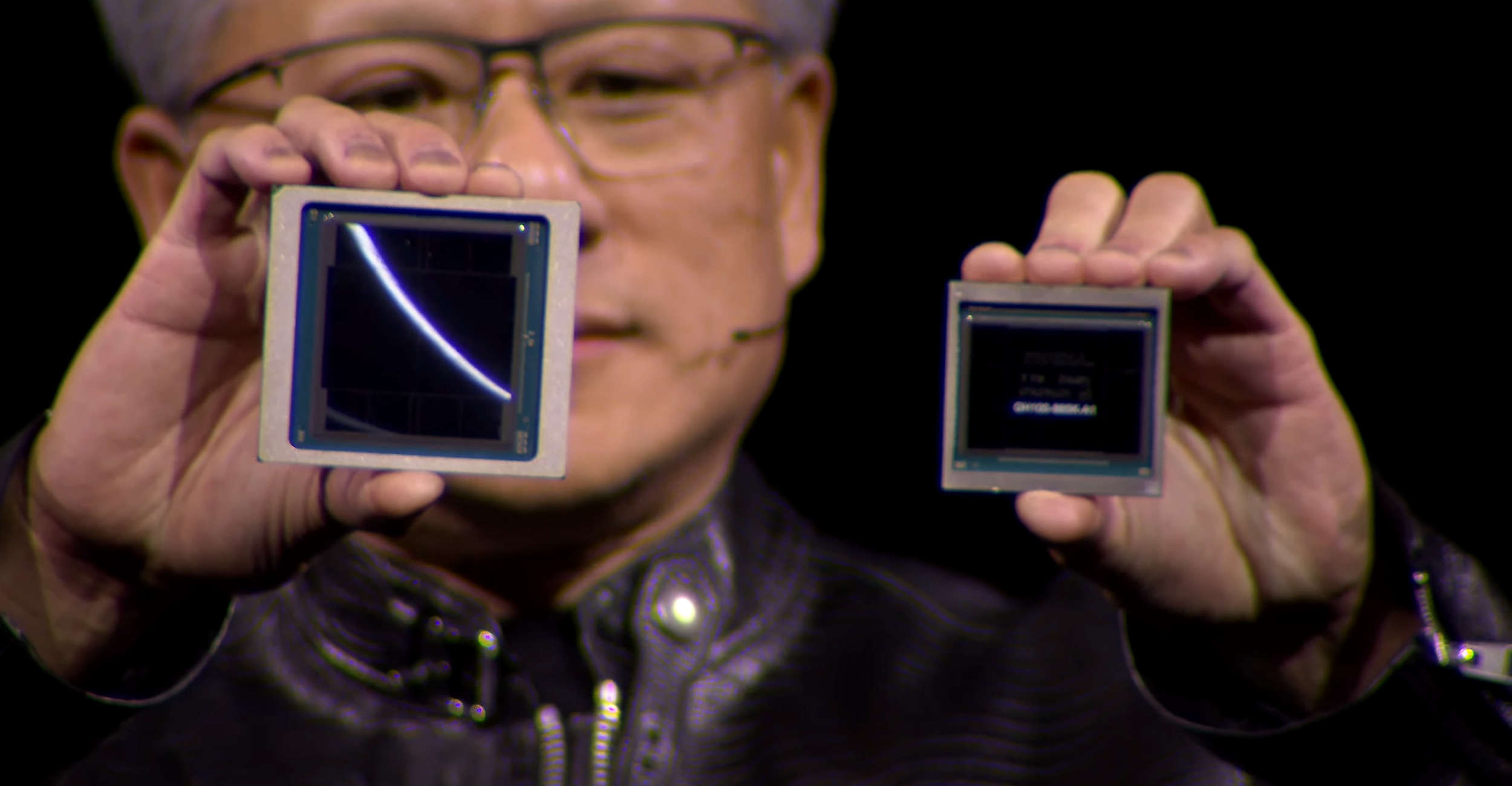
That's what lost me a little, normally his speeches are more put together and some elements felt phoned in. When they brought out the two Blackwell boards, it felt like that segment went on way too long and like he was expecting a bigger payoff for people's enthusiasm...Jensen Huang has already talked about so many PFLOPS that I don't care anymore for drake's performance LMAO
Interestingly, Blackwell has a decompression engine. Developed at the same time as Drake's or were they developed separately?
Yes I think the 50 series will also use N4P. My guess is that N3 yields are atrocious for large dies and thus MCM is the way to go to pack in more transistors vs. a node shrinkAssuming the rest of the Blackwell platform is on 4NP, do we think they're just gonna keep with it for the 50-series? Ampere datacenter chips were a node ahead of the 30-series, and Hopper was the same node as the 40-series, so maybe they don't see 3 nm as worth it and are just waiting for TSMC to switch to GAAFET for N2 and use that for Blackwell-Next?
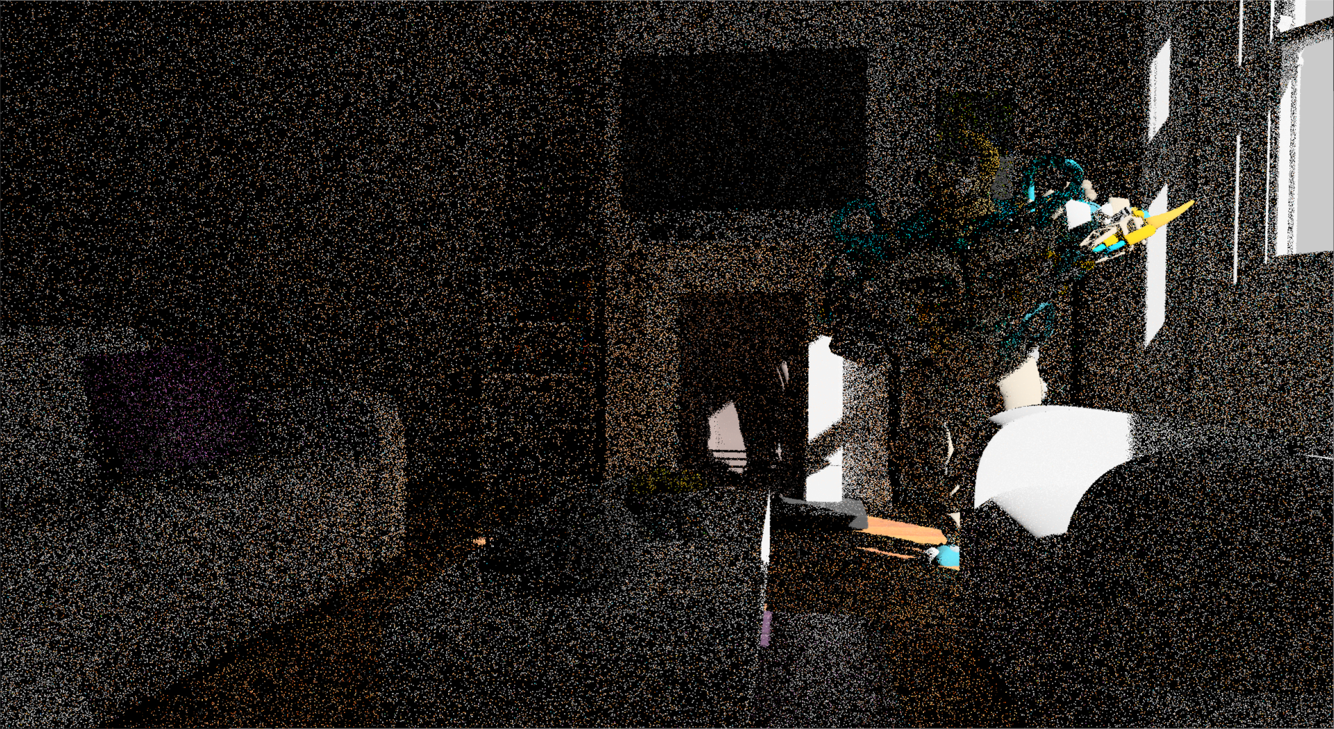
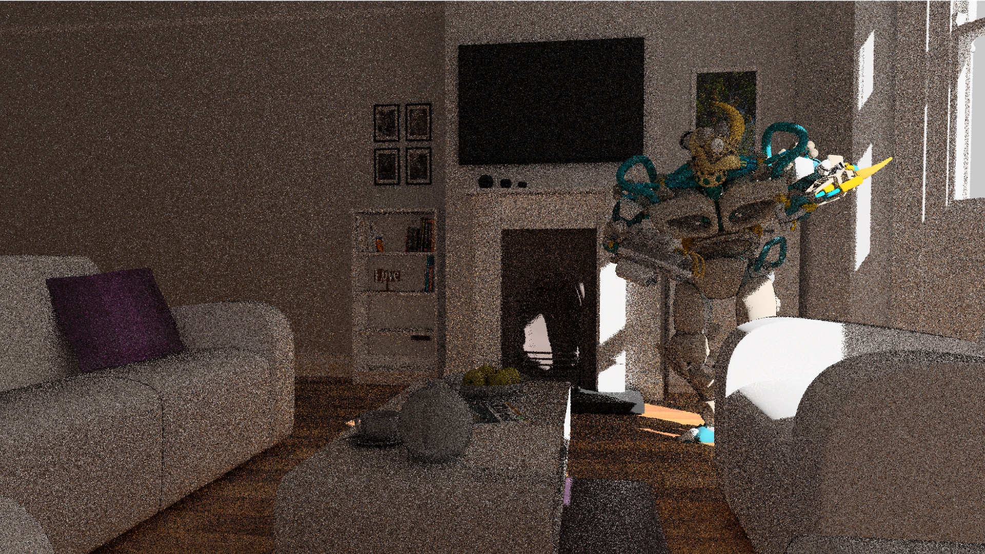
Neural Radiance Cache (NRC) is an AI-powered algorithm that trains the radiance cache about a scene in real time, handling fully dynamic scenes with no assumptions about lighting, geometry, and materials. It uses AI acceleration to train the radiance cache in real time to offer improved performance and more accurate global illumination in highly demanding scenes.
Spatial Hash Radiance Cache (SHaRC) is a radiance cache that's built on a spatial hash data structure designed for a fast and scalable global illumination technique for path tracing. It's similar to NRC, but it doesn't use a neural network. SHaRC will run on any DirectX or Vulkan ray-tracing-capable GPU.

 developer.nvidia.com
 gpuopen.com
Yes I think the 50 series will also use N4P. My guess is that N3 yields are atrocious for large dies and thus MCM is the way to go to pack in more transistors vs. a node shrink
it was supposed to be uploaded tommorow, today was a different oneWhere'd the video go?
Because AAA developers make their games for PC, PS and Xbox, most probably won't make day and date Nintendo releases. Just later ports. They have their priority platforms, and Switch 2 will be a bonus platform for them that comes later.You still havent adequately explained why you don’t think MH:Wilds can be a launch title, other than the condescending “you will be disappointment” (sic) take.
I’m not expecting MH:Wilds to be a launch title but I’m also not seeing anything that will prevent it from being one if that’s the plan
It depends. Some flavors are straight up enhacements over the original nodes and the OG node is basically phased/morphed into these nodes. Other times, they're just specialized versions of the nodes for specific applications and don't replace the OG node but rather are offered as alternatives depeding on your design target.Now I'm hoping for a 4NP Drake? See what you've done?!
More seriously, something I wanted to know - do "refinement nodes" of this kind that are essentially still just improved versions of the primary node (in this case TSMC 5nm) actually cost more money and see separate pricing for N5, N4, 4N, N4P, 4NP and N4X? Or are they just "this is what 5nm customers get now, for the same money per wafer"?
This is just the Switch to connect all these GPUs hahaha. Nvidia introduced compute capability so that the Switch is now capable of detecting reliability of each part of the connected GPUs and indicate if something is wrong.Aren't those tflops weak? 3.6 fp8 means only 0.9 fp32.
Unless I'm misunderstanding something? I wonder why that number with no mention of clocks. Is that max? I'm all over the place now
To me, it almost feels alien in the sense that: how did we as humans achieve this, and so fast?

We know the target power draw of the GPU for 2TFLOPs, 3.456TFLOPs and 4.236TFLOPs, while the GPU was designed.High performance on a nominally worse node means higher power consumption. I would go against the idea that this is purely academic or meaningless, even if we can "lock in" an expectation of 4TF (personally I wouldn't, but it does seem likely), the node discussion becomes the power discussion, becomes the size, the fan, the battery.
However in this case, you're right in a way still. Either they have gone with 4N, or have power optimised 8nm so much it doesn't matter. However, the risk remains that if it's 8nm, that means a big, hot, power hungry mess, and that would just be unfortunate.
Given Nintendo's MO, their success with handhelds and the sleekness, relatively speaking, of Nintendo Switch, this situation seems EXTREMELY unlikely, I think we agree there, but it's at least worth discussion something that could seriously change our expectations for form factor.
And if the form factor doesn't change despite 8nm, then yeah, that's expecting them to break physics.
Aren't those tflops weak? 3.6 fp8 means only 0.9 fp32.
Unless I'm misunderstanding something? I wonder why that number with no mention of clocks. Is that max? I'm all over the place now
Nvidia SHARP is a technology that puts a small amount of AI capacity in network devices. It's pretty weak for a GPU but pretty crazy for a network device.AFAIK the NVLink Switch is just to connect these multiple NVLinks, which in turn are used to connect multiples GPUs.
Considering how much Rise sold, Capcom would be absolute fools to not make the Switch 2 a "priority platform". Hell, Rise was a Switch exclusive for 10 months, so the MH team clearly see the value in supporting – and even giving special treatment to – Nintendo platforms when the technology is there, as they have since Tri.Because AAA developers make their games for PC, PS and Xbox, most probably won't make day and date Nintendo releases. Just later ports. They have their priority platforms, and Switch 2 will be a bonus platform for them that comes later.
There is nothing conflicting that this test was for target clocks and estimated power draw. It's actually the only thing they could reasonably be assumed to be. As for the hidden text, I agree that someone shouldn't quote your content without the hidden tag, but I'd rather fight the spread of misinformation, so I'll keep my posts and content open.* Hidden text: cannot be quoted. *
Hey, everyone. This may sound a bit off topic, but I wanted to ask the hardware experts here:
How has technology advanced so much?
Like, almost 60 years ago computers occupied entire rooms in order to process smaller sizes of information. Nowadays, nano sized hardware pieces process exponentially more data than what we had when we first started.
To me, it almost feels alien in the sense that: how did we as humans achieve this, and so fast?
And this is my question: how has technology advanced so much?
So Kopite7Kimi was right, he was also right that Blackwell is still N4,N4P
Huh, oh, right!We know the target power draw of the GPU for 2TFLOPs, 3.456TFLOPs and 4.236TFLOPs, while the GPU was designed.
So we don't have to worry about power consumption or clock. The node can be called anything, we know the specs. That's my point here, worrying about fighting over the actual process node is just for people who want to prove others wrong and there is no way of doing that with anyone who believes these performance numbers are possible on 8nm. My secret point is that they lack understanding needed to argue in good faith.
kopite7kimi also said that T254 was based on Blackwell, which is likely wrong since Thor is likely T264, not T254.So Kopite7Kimi was right, he was also right that Blackwell is still N4,N4P
They will use N3 but in 6000 series, if Blackwell gaming is Early 2025, then 6000 series can be Early 2028Assuming the rest of the Blackwell platform is on 4NP, do we think they're just gonna keep with it for the 50-series? Ampere datacenter chips were a node ahead of the 30-series, and Hopper was the same node as the 40-series, so maybe they don't see 3 nm as worth it and are just waiting for TSMC to switch to GAAFET for N2 and use that for Blackwell-Next?
N3 and N2 dosent sucks at all, maybe if you mean prices then okI mean, 3nm just fucking sucks so maybe.
(2nm sucks worse, not looking good)
* Hidden text: cannot be quoted. *
You can't just say they can "reasonably be assumed to be" something without justifying your interpretation.There is nothing conflicting that this test was for target clocks and estimated power draw. It's actually the only thing they could reasonably be assumed to be. As for the hidden text, I agree that someone shouldn't quote your content without the hidden tag, but I'd rather fight the spread of misinformation, so I'll keep my posts and content open. Switch 2 is a 3 to 4 TFLOPs device and those clocks from the test are not in any conflict from being used on Switch 2 by us or MLID, the idea that we then have to prove it isn't 8nm, well that's obvious to anyone you could prove it to with these numbers, but I'll refrain from that argument.
Moore's law, and Math.Hey, everyone. This may sound a bit off topic, but I wanted to ask the hardware experts here:
How has technology advanced so much?
Like, almost 60 years ago computers occupied entire rooms in order to process smaller sizes of information. Nowadays, nano sized hardware pieces process exponentially more data than what we had when we first started.
To me, it almost feels alien in the sense that: how did we as humans achieve this, and so fast?
And this is my question: how has technology advanced so much?
You found the test and shared it with the community, if you look at my posts where I use your name, I do say that my conclusion is in conflict with yours. Now these tests were done in summer 2021, when there was no card that could match the test's configuration.You can't just say they can "reasonably be assumed to be" something without justifying your interpretation.
There is no reason to use T239 target clocks on a different GPU on Windows. There's literally no value to doing that. You might as well use a random number generator for how meaningful those clocks would be in the test. Using clocks that are relative to each other similar to the (not-yet-existent) handheld and docked profiles means that you'll get execution times distinct from each other, which makes looking at your results more intuitive, and that's the reason why the clocks are different at all. Beyond that, they're arbitrary.
The tests were KPI profiling of DLSS execution under NVN2. That means they needed to keep everything the same between runs so that any change in the output metrics -- execution time, memory usage, and image tests -- could be tracked as they made changes to the code. They wanted to see improvements and guard against regressions. That code is what was being tested, not clocks, not power consumption, not T239. The resolution, quality mode, and P-State are relevant for exercising the code paths closely to what T239 would do, but the clocks are not relevant because they have zero effect on how the test executes, only how fast it executes. And how fast or slow the test runs is meaningless in absolute terms, only relative ones. But even if you hypothetically wanted the absolute time to match T239 for some reason, you would not be able to accomplish that by applying its clock speeds to a random RTX 20 series GPU.
I could go on. We could talk about how timeline-wise, T239 didn't even physically exist at the time of the hack, and the test cases could have been written months or years earlier on top of that. But I've already made enough of an argument. If you want to keep going around telling people that these are T239 clocks -- invoking my name, no less -- then you really need to offer an argument for why they would use T239 clocks in these tests in light of everything I've laid out here. My belief is that the best possible argument one could make is "they did it arbitrarily," which is pretty weak, but I guess better than having no argument at all.
And then once VLSI came along, suddenly, computers were used to design computers. And fucking Xerox were the ones to do it because IBM were a bunch of transphobic cunts.Moore's law, and Math.
The guy (I believe his name was Cain) who discovered Rock did more than just think of a cool way to kill people. Rock could be used to make Sharp Rock. Sharp Rock could be made into knives, knives could be attached to Stick (older technology) to make Spear, Spear could be made small to make Arrow. Sharp Rock could also be turned into Axe, Axe could fell tree, Tree plus Rock could become Trebuchet.
The early discovery of a new class of technology always leads to rapid innovation, as there are lots of obvious and untapped applications. But this era of innovation can be intensified if the new technology can be used to refine itself. Rock can be used to make better Rock.
The transistor was not just a new class of technology, but it was one that had an obvious technological improvement - make it smaller. And how would you do that? With a whole bunch of automation made possible by... the transistor.
This lead to 30 years of increasing power, simply by riding the node shrink. Which is not to be dismissive of the electrical engineers and physicists who worked hard to make this possible, but the fact that Gordon Moore was able to chart three decades of technological progress pretty accurately shows that it was an era of low hanging fruit.
Along the way came Math - Math is obviously thousands of years old, and the basis of software is Math. The neural network is 81 years old, but practical software applications didn't exist until we made powerful enough GPUs. The math was waiting there for the hardware to catch up. There have been huge advances in the field of software engineering, and of course, advances in Math - but again, Ada Lovelace wrote the first program well before the first computer. These things were ready to go the moment Electronic Math Machines were viable.
So the reason computers got so good so quickly is MinecraftRock could be used to make Sharp Rock. Sharp Rock could be made into knives, knives could be attached to Stick (older technology) to make Spear, Spear could be made small to make Arrow. Sharp Rock could also be turned into Axe, Axe could fell tree, Tree plus Rock could become Trebuchet.

dammiSo the reason computers got so good so quickly is Minecraft
this was a typo, but I like it as a fami related sweardammi