• Hey everyone, staff have documented a list of banned content and subject matter that we feel are not consistent with site values, and don't make sense to host discussion of on Famiboards. This list (and the relevant reasoning per item) is viewable here.
  • Do you have audio editing experience and want to help out with the Famiboards Discussion Club Podcast? If so, we're looking for help and would love to have you on the team! Just let us know in the Podcast Thread if you are interested!

StarTopic Future Nintendo Hardware & Technology Speculation & Discussion |ST| (Read the staff posts before commenting!)

One thing worth clarifying, the TSMC N4 process, used for the iPhone 14 Pro, isn't the same as the 4N process, used for the Nvidia 4000 series GPUs. The latter is a "customised" process for Nvidia which is rumoured to be based on N5P process. The "Xnm" names foundries give to manufacturing processes have long since diverged from reality, so Nvidia likely just wanted to call it 4N so that people would think they're on a more advanced node than AMD, even though they're likely on a basically identical process.

Secondly, the difference between N5, N5P, N4 and the confusingly named 4N doesn't really matter that much. They're all part of TSMC's 5nm family of manufacturing processes, and are largely the same process, with relatively minor differences in density, performance and power. They're made on the same manufacturing lines, and a design could probably migrate from one to another relatively easily (not that there's much point). TSMC just started calling it 4nm because it sounds better, neither N4 or 4N are actual new manufacturing processes like N5 was or like their 3nm processes will be. If Drake does use a process in the TSMC 5nm family, it would almost certainly be the 4N variant, as that's what Nvidia's using for everything else. (Also I believe the first N4 chip was the MediaTek Dimensity 9000, which was in shipping products earlier this year).

The TSMC 5nm family as a whole isn't as new, as expensive, or in as short supply as many people think. In terms of timing, the first TSMC 5nm chips arrived in products toward the end of 2020. With an early 2023 launch, that would put the 5nm family at 2 and a half years old, pretty much exactly the age that 20nm was when Switch launched, and a bit older than the 7nm family was when PS5 and XBSS/X launched. In fact, the new Switch model will be in a very similar position to the PS5/XBS, as TSMC's new 3nm process will be hitting products at around the same time as the new Switch hardware, similar to PS5/XBS launching at around the same time as the first 5nm products.

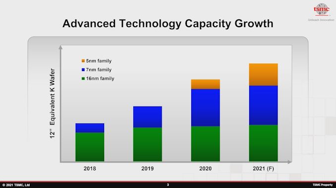
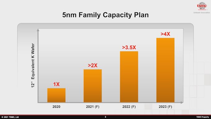
In terms of supply, TSMC's 5nm family has some of the highest wafer capacity of any manufacturing process, and accounting for transistor density may actually have the highest capacity in terms of how many chips it could produce. Take a look at these graphs provided by TSMC from this Anandtech article last year:

Manufacturing%20Excellence%201.mp4_snapshot_00.51_%5B2021.06.01_20.43.13%5D_575px.jpg

Manufacturing%20Excellence%202.mp4_snapshot_00.49_%5B2021.06.01_20.43.32%5D_575px.jpg


TSMC's plan was for the end of 2022 to have almost as much wafer capacity for their 5nm processes as their 7nm processes, likely overtaking 7nm shortly after. Obviously these were forecasts, but it's unlikely they slowed down in the past year. It's an extremely high volume manufacturing process, and we know that Nvidia has already paid TSMC a large amount of money for a signifiant allocation of it.

In terms of price, we can't say for sure what TSMC charges for its wafers, but they do split their revenue by process, so we can make some reasonable estimates about the relative cost of the wafers. From their Q2 investor report (slide 4), we know that 21% of their their revenue was from 5nm processes, vs 30% for 7nm processes. From their projections above, we would expect 5nm capacity to be about 60% of 7nm capacity in early 2022, which combined with the reported revenue, would mean their revenue per wafer is... about the same. This obviously isn't quite right, and it's possible that 5nm expansion is a bit behind schedule, or they've expanded 7nm more than expected. There's also probably a bit of a lag between capacity coming online and TSMC seeing revenue from it. Still, the revenue and capacity information provided by TSMC are inconsistent with the notion that their 5nm family is massively more expensive than 7nm on a per-wafer basis, and it would have to be massively more expensive on a per wafer basis to be more expensive on a per-chip basis.

How massively more expensive? A while back I did some rough estimates of chip costs on different processes, assuming an 8 billion transistor chip. For TSMC 6nm, that came to 112.8mm2 by my estimates, which would mean 530 would fit on a wafer, per this online calculator. With a defect rate of 0.1 per cm2, that would yield an average of 470.6 working dies per wafer. On TSMC's "4N" process, with the Ada GPUs, Nvidia is hitting between 121.1 and 125.5 million transistors per mm2. Using 121.1, that would put an 8B transistor Drake at 66.1 mm2. That would mean 916 would fit on a wafer, and with the same defect rate of 0.1, it would yield an average of 866.9 working dies per wafer.

What this means is that TSMC would have to be charging 84% more for a 5nm wafer than a 7nm wafer, just for them to be the same price per die in this case, ignoring any benefit in terms of clocks or power efficiency. Judging by the data above, it seems very unlikely to me that TSMC are charging that much for a 5nm wafer. If that was the case we'd be seeing 5nm revenue being around the same, or even overtaking 7nm revenue, which isn't the case. The 5nm family is certainly more expensive per wafer than the 7nm family, but the evidence suggests it's actually cheaper per chip, even ignoring the benefits in terms of power efficiency, which would be especially important for a device like the Switch.

Finally, the most important thing to note is that Nintendo and Nvidia aren't making this decision in 2022 with the data available to us now, they made the decision back when work started on the chip, likely in late 2019 or early 2020. That was pre-covid and pre chip shortage. Around that time Nvidia would have also been making the same decision for chips like Hopper and Ada and Grace, and in all of those cases they seem to have gone for TSMC's 5nm family. Rumours also suggest that even the entry-level chips in the Ada family (ie the RTX 4050, etc.) are being manufactured on the same N4 process, and these are likely to release at around the same time as the new Switch model. If they did choose TSMC's 5nm family for Drake, then it already would have been included in the billions of dollars they paid TSMC to reserve capacity on the process.

This isn't to say I think that Drake is certainly on the N4 process. R&D costs could have come into it with Ampere on 8nm and 7nm processes, and perhaps TSMC's 5nm capacity projections weren't quite that aggressive back in 2019/2020. But I certainly wouldn't rule N4 out, either.
Another thing to add to this is Nvidia does have AI fab tech that allows them to shrink dies faster and we did hear about "Dane" code name for T239, that happened to be magically word blocked in the Nvidia hack, it's possible they did a die shrink whenever brainchild mentioned some power issues in early 2021.
 
Another thing to add to this is Nvidia does have AI fab tech that allows them to shrink dies faster and we did hear about "Dane" code name for T239, that happened to be magically word blocked in the Nvidia hack, it's possible they did a die shrink whenever brainchild mentioned some power issues in early 2021.

To add a little more, Nvidia could have predicted their reduced GPU demand as early as Q1 2021 as it was already known that etherium was moving to a proof of stake model and the negative sentiment towards mining was on the rise, so they may have already known their 4N capacity they reserved was going to be under utilised by their traditional GPU market. Or like you said 8N samples of "Dane" had serious issues with power consumption and heat so they shrank it.

Might even explain the OLED models existence.
 
Last edited:
To add a little more, Nvidia could have predicted their reduced GPU demand as early as Q1 2021 as it was already known that etherium was moving to a proof of stake model and the negative sentiment towards mining was on the rise, so they may have already known their 4N capacity they reserved was going to be under utilised by their traditional GPU market. Or like you said 8N samples of "Dane" had serious issues with power consumption and heat so they shrank it.

Might even explain the OLED models existence.
I'd stop shy of OLED model, Drake was a 2022 holiday or 2023 spring model since 2020
 
There are plenty of games with Switch and PS4 versions. This wouldn't be so dissimilar.
while that is true, the difference here is that a game like Tears of the Kingdom is already sort of designed for Switch (and a derivative work based on tech designed for Wii U/Switch) so I imagine comparing the game running on the switch and also running on this theoretical new piece of hardware wouldn't be as drastic as comparing a game designed for PS4 that had been scaled down to run on switch.

Sure the new version would be running at a higher framerate and resolution, but I think they would need to do a bit more in order for it to seems like a worthwhile upgrade for many consumers.

This is just a different situation as the transition from Gamecube -> wii and wii u -> switch because nintendo needs to sell this new console to current switch owners as well, whereas for those previous transitions they were trying to sell the console to people who didn't buy the previous one.
 
Quoted by: MP!
1
I'd stop shy of OLED model, Drake was a 2022 holiday or 2023 spring model since 2020

Yeah sorry, I keep forgetting that part.

I do wonder how much of the OLED components they will use for Drake though. Naturally things like storage, motherboard, RAM etc are off the table. But display, Dock and power supply is possible. Actually if the funcles leak about vent placement being different has weight then the dock is also off the table.

It always felt a strange product to me, like Nintendo must have had some other reason for putting it together, but I guess the proof is in the pudding and it's now shifting the most units.

Could be they reuse the display and the OLED was a way of ramping up OLED display volumes before Drake launched, a way to ease that possible bottleneck, or the product could have been a test of consumer sentiment towards a premium switch product.

Or I'm overthinking because I am so damn hyped for Drake to launch.
 
I wonder how android supports different types of GPU and not break compatibility as far back as android 4.0.
By making it extremely slow.

First off, the majority of Android development happens in Java/Kotlin. They're not even written in a compiled language, they're just shipping around bytecode that gets JITed on startup.

But the primary reason - apps don't have access to the hardware at all, they don't even have direct access to the driver.

Android offers an API like OpenGL ES for doing 3D graphics - an API designed 20 years ago on top of previous API designed 30 years ago. Applications are written against that library.

Applications are loaded by the kernel into userspace, and the shared library for OpenGL is mapped into memory, and addresses are rewritten in the application's memory to match their actual locations.

The application calls an OpenGL routine, which walks into the shared library. The OpenGL routine performs whatever userspace logic is required, and then needs to send commands to the hardware. Userspace doesn't have direct access to hardware for security reasons, so the OpenGL routine uses system calls to communicate with a generic interface on the kernel.

This causes a context switch, where the entire applications state is suspended for later resumption, control passes into the kernel which passes control into the driver which implements the request, control passes back up to the generic wrapper in the kernel who restores the application's state, and resumes executing inside the shared library which performs and additional logic required.

If the OpenGL routine requires multiple commands to the hardware that cannot, in some way, be batched, this application suspend, context switch, kernel->driver->kernel operation happens every tie.

Then, the library returns, control is restored to the application, which then calls it's next OpenGL command.

The application knows nothing about the hardware and has two layers with heavy security checks between them and said hardware, while working with an inefficient interface to do it.

Context switches are very slow, OpenGL ES is extremely abstract and inefficient, and apps and games are poorly optimized to the hardware or at best optimized to only a few elite phones.

Here's hoping switch's library is platform agnostic and highly abstracted.
It is the exact opposite. It is minimally abstracted and highly specific. And that is what you want

First, they don't use OpenGL. They use NVN. NVN is a modern API designed at the same time the hardware was. Also, NVN is thin. It expects that the user can handle building complex 3D scene graphs themselves, and it just gives you access to the hardware to do it. Plus it encodes specific data about the hardware to do it, because that version of NVN is built for one piece of hardware and one piece of hardware only. Games can bake in assumptions about the amount of memory or number of compute units available.

Actually, they can use OpenGL, Nintendo provides tools to do it. And in practice, games don't get hyper optimized to the GPU, they leave that to the engine. In modern game development, the engine is the important abstraction layer where performance optimizations occur, not the lower level libraries.

This makes it blazingly fast, and allows game devs to perform optimizations not possible in Android. But above and beyond that, the context switch is eliminated, as is the shared library penalty.

NVN isn't just the API, it is the driver. In older OSes this was often the case when the "driver" was really just "that vendor's implementation of OpenGL/DirectX", but security makes that a Bad Idea for generic devices. A gaming console isn't a generic device, and can eliminate whole classes of security concerns. The game and the OS are the only thing running. You don't have 50 tabs open in a browser, one of which is logged into your bank and all of which can execute arbitrary javascript. Game consoles can afford to give you direct access to the raw hardware, without passing through the kernel to do it.

And it isn't implemented as a shared library, either. Unlike on Android, where an application ships to you and then asks the OS for it's implementation of OpenGL, instead it brings its own, hard linked into the game binary.

So to sum up, on Android where start up and initial draw call to paint a "Built on Unreal" logo to the screen would go like this...

Read game byte code->recompile byte code to machine code->load openGL libraries->map game addresses for openGL functions into application memory->run game's main()->game calls openGL init->game creates openGL surface->call kernel->save application state for resumption->call driver->driver provides pointer to GPU memory->kernel validates pointer, randomizes the underlying address, passes it back to openGL library->resumes application state->OpenGL returns->app copies Unreal logo from it's memory onto provided GPU memory->call draw call on surface->go to kernel->save application state for resumption->call driver->driver draws the Unreal logo stored in GPU memory->return to kernel->restore state->open GL returns->back to game main()->okay, now to fade that logo out...

That's 24 steps, some of which (the context switching and writing into GPU memory) are extremely slowl. And on Switch with NVN...

Read game binary data->start game main()->GPU memory is main memory, just put logo in memory somewhere->game talks to GPU directly "Draw what's at this address"

4 steps, all of which are pretty quick.

This is one of the ways that game consoles are able to get within spitting distance of gaming PCs at sometimes as little as a tenth of the price. If NVN were "high level and extremely abstracted" then there would be no game console in the first place, you'd just run your games on cheap Android tablet.
 
By making it extremely slow.

First off, the majority of Android development happens in Java/Kotlin. They're not even written in a compiled language, they're just shipping around bytecode that gets JITed on startup.

But the primary reason - apps don't have access to the hardware at all, they don't even have direct access to the driver.

Android offers an API like OpenGL ES for doing 3D graphics - an API designed 20 years ago on top of previous API designed 30 years ago. Applications are written against that library.

Applications are loaded by the kernel into userspace, and the shared library for OpenGL is mapped into memory, and addresses are rewritten in the application's memory to match their actual locations.

The application calls an OpenGL routine, which walks into the shared library. The OpenGL routine performs whatever userspace logic is required, and then needs to send commands to the hardware. Userspace doesn't have direct access to hardware for security reasons, so the OpenGL routine uses system calls to communicate with a generic interface on the kernel.

This causes a context switch, where the entire applications state is suspended for later resumption, control passes into the kernel which passes control into the driver which implements the request, control passes back up to the generic wrapper in the kernel who restores the application's state, and resumes executing inside the shared library which performs and additional logic required.

If the OpenGL routine requires multiple commands to the hardware that cannot, in some way, be batched, this application suspend, context switch, kernel->driver->kernel operation happens every tie.

Then, the library returns, control is restored to the application, which then calls it's next OpenGL command.

The application knows nothing about the hardware and has two layers with heavy security checks between them and said hardware, while working with an inefficient interface to do it.

Context switches are very slow, OpenGL ES is extremely abstract and inefficient, and apps and games are poorly optimized to the hardware or at best optimized to only a few elite phones.


It is the exact opposite. It is minimally abstracted and highly specific. And that is what you want

First, they don't use OpenGL. They use NVN. NVN is a modern API designed at the same time the hardware was. Also, NVN is thin. It expects that the user can handle building complex 3D scene graphs themselves, and it just gives you access to the hardware to do it. Plus it encodes specific data about the hardware to do it, because that version of NVN is built for one piece of hardware and one piece of hardware only. Games can bake in assumptions about the amount of memory or number of compute units available.

Actually, they can use OpenGL, Nintendo provides tools to do it. And in practice, games don't get hyper optimized to the GPU, they leave that to the engine. In modern game development, the engine is the important abstraction layer where performance optimizations occur, not the lower level libraries.

This makes it blazingly fast, and allows game devs to perform optimizations not possible in Android. But above and beyond that, the context switch is eliminated, as is the shared library penalty.

NVN isn't just the API, it is the driver. In older OSes this was often the case when the "driver" was really just "that vendor's implementation of OpenGL/DirectX", but security makes that a Bad Idea for generic devices. A gaming console isn't a generic device, and can eliminate whole classes of security concerns. The game and the OS are the only thing running. You don't have 50 tabs open in a browser, one of which is logged into your bank and all of which can execute arbitrary javascript. Game consoles can afford to give you direct access to the raw hardware, without passing through the kernel to do it.

And it isn't implemented as a shared library, either. Unlike on Android, where an application ships to you and then asks the OS for it's implementation of OpenGL, instead it brings its own, hard linked into the game binary.

So to sum up, on Android where start up and initial draw call to paint a "Built on Unreal" logo to the screen would go like this...

Read game byte code->recompile byte code to machine code->load openGL libraries->map game addresses for openGL functions into application memory->run game's main()->game calls openGL init->game creates openGL surface->call kernel->save application state for resumption->call driver->driver provides pointer to GPU memory->kernel validates pointer, randomizes the underlying address, passes it back to openGL library->resumes application state->OpenGL returns->app copies Unreal logo from it's memory onto provided GPU memory->call draw call on surface->go to kernel->save application state for resumption->call driver->driver draws the Unreal logo stored in GPU memory->return to kernel->restore state->open GL returns->back to game main()->okay, now to fade that logo out...

That's 24 steps, some of which (the context switching and writing into GPU memory) are extremely slowl. And on Switch with NVN...

Read game binary data->start game main()->GPU memory is main memory, just put logo in memory somewhere->game talks to GPU directly "Draw what's at this address"

4 steps, all of which are pretty quick.

This is one of the ways that game consoles are able to get within spitting distance of gaming PCs at sometimes as little as a tenth of the price. If NVN were "high level and extremely abstracted" then there would be no game console in the first place, you'd just run your games on cheap Android tablet.
That's quite an impressive read. Thanks for shining light to the issue.
 
I know this has pretty much already been answered, but would a Drake Pro/ New Drake even be possible in 2025? Just purely to entertain the "but the real next-gen Switch is probably coming out two years later, in 2025!" people. Regardless of whether or not it makes sense from Nintendo's perspective, if such a thing were true, we would have heard rumors about another set of dev kits going out right? But let's say they rush it out. Is Drake pro or Switch "3" achievable in 2025 (again I don't believe this is happening at all, but just as a 'what if')
There could be a new SOC based on Atlan in theory, but it definitively wouldn’t be a “next gen” leap over Drake.
 
It always felt a strange product to me, like Nintendo must have had some other reason for putting it together, but I guess the proof is in the pudding and it's now shifting the most units.
Nintendo refreshes their handhelds. The strategy for Switch has been the strategy they've used for the handheld lines forever, it just seems stranger in the context of the "big" consoles. Refreshes drive sales of handhelds in a way they don't for big TV consoles, because people are more willing to "upgrade" a device they hold in their hand all the time for minor reasons, and reselling your handheld to the secondary market is much easier than detangling your entire entertainment center to sell the Absolute Unit that is a modern TV console.

The refresh rate for the Switch actually seems kinda low relative to previous handhelds, but the higher price tag and the need to project "premium" probably drives that. DS got the DS Lite, which was basically "it looked nicer and the screen was a little brighter" and every single DS owner I know upgraded eventually - which is how I was able to afford a DS in the first place, because I could buy them used.

Look at these dates
2001: GBA
2003: GBA SP
2004: DS
2005: GB Micro
2006: DS Lite
2008: DSi
2010: DSi XL
2011: 3DS
2012: 3DS XL
2013: 2DS
2014: New 3DS
2015: New 3DS XL
2017: New 2DS XL and Switch
2019: Switch Lite
2021: Switch OLED

15 handheld variants over 20 years, a new handheld every 16 months, and the basic strategy is to release some sort of "premium" and "your kids won't break it, entry level" device for every one before moving on to the "next" hardware.

It's not a clockwork strategy, of course. Depending on how you slice it, the DS got 1 revision or 3, and that was in response to the Vita. The GBA and the N3DS both had a revision launch after their successor, but in both cases this was Nintendo's "3rd pillar" strategy, where they were leaving a window open to jump back to a previous handheld line if the different formfactor successor didn't take off.

But looked at this way you can pretty clearly see Nintendo's strategy. Release a handheld console, do a refresh that makes it more "premium" or more "adult" for users who have scuffed up their original and/or didn't want to be seen in public carrying around what looked like a toy, and do a refresh that possibly sacrifices a key selling point of the device (A switch that can't switch, a 3DS with no 3D, a game boy that can't actually play original game boy games) in order to make it cheaper and have fewer moving parts for kids to break.

Nintendo also likes to hold on to their handheld brand for a long time. When I was a kid the NES/SNES/N64 were all "Nintendos" but the GameBoy was a "gameboy." It had it's own brand and from the virtualboy to the gameboy advanced, Ninty held that brand (and backwards compat, mostly) until they were sure that the DS line was gonna have legs. And while the 3DS was it's own "family" the base DS brand held for 13 years, with the New3DS XL still having a DS slot for backwards compat.

This doesn't make hardware like Drake inevitable, but we're pretty much on schedule for a Next Switch, with backwards compat and some period of cross gen until the new device gets its sea legs, and the OLED model doesn't stick out in that regard, it seems very much par for the course.
 
0
I know this question already has been discussed a lot, but what is the opinion around here on how they'll do backwards compatibility?
Completely new chip means that games need to be adapted and tested, will Nintendo do that by themselves similarly like Microsoft?
Updating games shouldn't be super time consuming, because of evolution of software (NVN2) and hardware, but then it could still be possible that quite a few Switch games aren't ready at launch for Drake.

Or do you think that they'll go a different route, like including the Tegra X1 in the new chip?
They don't have to change everything, they just need adequate emulation of the original Maxwell GPU. I'm expecting it will primarily involve some binary translation in the graphics driver (the part that's actually in the OS), with probably a few other assorted compatibility adjustments for a few non-graphics things.
I wonder how android supports different types of GPU and not break compatibility as far back as android 4.0.

Here's hoping switch's library is platform agnostic and highly abstracted.
Console games typically skip a few steps to go faster that are traditionally required in more hardware agnostic environments. This directly exposes them to certain thorny implementation details that are dealt with by the driver on other platforms, most relevantly that, unlike CPUs, GPU instruction sets are not at all stable between generations. Shipping games with shaders precompiled for specific GPUs is completely infeasible on a more open platform, but consoles can get away with it because there's only one GPU to worry about.
I know this has pretty much already been answered, but would a Drake Pro/ New Drake even be possible in 2025? Just purely to entertain the "but the real next-gen Switch is probably coming out two years later, in 2025!" people. Regardless of whether or not it makes sense from Nintendo's perspective, if such a thing were true, we would have heard rumors about another set of dev kits going out right? But let's say they rush it out. Is Drake pro or Switch "3" achievable in 2025 (again I don't believe this is happening at all, but just as a 'what if')
Nvidia's Atlan SoC will in theory be available by then. If a device using an SoC derived from that is happening, we'd likely start hearing rumblings of it at some point next year at the earliest.

That said, we'll see how Lovelace performs compared to Ampere, but it's likely to be a far more modest upgrade from Drake than Drake is to TX1.
 
Nice to meet you.
I was surfing the net and found the following information. What do you think?
I haven't analyzed the article in detail, but (unless Firefox's translator is way off) the article appears to be claiming two CPU clusters, which is in direct contradiction with some of the code Nvidia recently contributed to the Linux kernel that appears to indicate only one cluster.
 
Nice to meet you.
I was surfing the net and found the following information. What do you think?
It says here the screen is known to be HDR at Full HD resolution. Full HD usually means 1080p, which I'm skeptical of. I would have assumed they'd be reusing Switch OLED panels. Maybe it's just the resolution of a devkit display.

This is also saying DLSS is only used in docked mode. No DLSS in handheld mode + 1080p screen sounds not great to me, tbh.
 
Yeah, I think that article is probably fake. Parts of it seem plausible, but other parts of it seem a bit sus (like the whole getting rid of explicit docked and portable mode thing) and there's at least one contradiction with public info that doesn't seem like a plausible mistake.
 
The article you are reading is an updated version of what I shared on Discord a few weeks ago, so there is much more information than you saw in that archive. This is still just a temporary overview of the hardware of the potential Switch 2, Nintendo's next-generation console that will replace the current Nintendo Switch in the market.

The Switch 2's main chip

The main chip of the console has been designed by NVIDIA, it is unknown which manufacturing node Nintendo and NVIDIA have opted for, at first it was going to be manufactured under TSMC's N7 node, but everything points to the choice being the N6 node. The SoC is completely custom, so it will not be used in any product other than Nintendo's next console and is codenamed T239.

We know this from NVIDIA's leaked documentation a few months ago from the attack on their lapse servers. Thanks to this we were able to know that the T239 is the chip of the Nintendo Switch 2 by being related to the NVN2 API. Remember that NVN is the Nintendo Switch graphics API, so this would be an improved version of the one used in Switch.

Coprocessors

However, despite being derived from the Tegra, which are now automotive-focused, a good part of the coprocessors included for it have been discarded in the process, so the only ones included in the chip, apart from the CPU and GPU are:

The chip can play video in all kinds of formats, including AV1. It actually inherits from the Tegra Orin its NVDEC. Unfortunately, Nintendo has taken away its ability to encode video through NVENC.
The Audio Processor Engine or APE is in charge of audio processing on the Tegra and therefore the music and sound libraries of the games depend on it. So it is obviously a unit that is maintained.
The VIC or Video Integrated Controller is the one that reads the image buffer and transmits it through the video signal to the display. Whether it is the console's own display or an external TV.
The chip contains temperature sensors that act in conjunction with the coprocessor responsible for carrying out the control of the system. This coprocessor is important in Switch 2 and is responsible for handling the following parameters:
The frequency and voltage of the CPU and GPU.
The number of active cores at any given time.
To turn coprocessors on and off when they are not in use.
A final coprocessor is a DMA unit with on-the-fly data compression and decompression for transfer between storage and RAM and vice versa.
Clock frequencies and CPU-to-GPU ratio

In Switch 2 the concept of Dock mode and Undock mode (portable) has completely disappeared, the console has adopted the same concept as NVIDIA's Max-Q/Max-P that AMD would later copy in the form of Smartshift, which went to PS5, and, therefore, we are talking about clock rates being dynamic and not static. The coprocessor in charge of keeping track of the system takes the different values depending on the load level in the game.

If the CPU is on high, then the GPU is set to low.
On the other hand, if the GPU is on high, then the CPU is set to low.
There is a balanced mode where both run at medium speed.
When we are browsing the console menu or in the eShop, the system is designed to use only 2 CPU cores at the lowest supported speed and the GPU with most of its cores disabled except 2 SM and also running at the lowest possible speed. The first CPU core controls the operating system and is isolated from the rest, the second one is in charge of handling the menu environment and when we load a game this environment remains in the background in the system RAM.

The number of GPU SM cores and CPU cores can be disabled when they are not needed. This is not done by the game code, but if a part of the chip is unused, it is immediately de-energized. It is precisely the part in charge of battery life that they have optimized the most, so games do not use 100% of the hardware all the time.

The CPU

The core processor is two full Cortex A78E clusters of four cores each, all with a 2 MB L2 cache per cluster. So we have a total of 8 cores. Nintendo and NVIDIA have not placed any additional support processors in the form of e.g. the A55. The processor also does not support multithreading.

Its power is higher per clock cycle than PS4 and Xbox One CPUs, but it is a far cry from those of the current generation. Moreover, in Switch backwards compatible mode it runs in a limited way at 1020 MHz and using only 4 cores. In contrast, in Switch 2 mode it has 3 clock speeds that depend on the workload at the time.

L3 cache

The Switch 2 SoC has 4 MB of third level cache, which is located before the memory controller and is responsible for making all RAM accesses between CPU and GPU coherent and that these can also pass messages to each other without passing through RAM. This reduces power consumption and communication latency. In backward compatible mode this cache is not used and is completely disabled.

GPU

The graphics processor in Switch 2 was designed with the recently released RTX 30, so its SM cores are exactly the same as you can find in the RTX 30. Actually the internal name of it is GA10B and a trimmed version of the RTX 3050.

I have made a quick diagram so you can get a visual idea of it, which is much easier to understand


Descriptively, the Switch 2 GPU has the following features:

Unlike Switch's TX1 where we only had one GPC, we now have two, so the number of raster triangles per clock cycle has doubled.
The number of GPU cores, SM in NVIDIA slang, is now 12.
Each SM has the same configuration as NVIDIA's RTX 30 and RTX 40.
That is: 64 ALUs in FP32 + 64 ALUs FP32/INT32 switched. This makes 1536 32 bit floating point units.
Twice as many as Xbox One.
50% more than PlayStation 4
3 times more than Steam Deck.
Inside each SM has the corresponding Tensor units to perform the NVN DLSS, a variant of the PC DLSS 2 optimized for the Nintendo Switch 2.
NVN DLSS is only used in dock mode, where the GPU is set to a higher clock speed to trigger the algorithm and scale from 1080p to 4K.
If the connected TV is Full HD then NVN DLSS is not activated.
At the moment, neither Nintendo nor NVIDIA have found a single Switch game that requires the use of DLSS to run at Full HD resolution and 60 FPS.
Unlike the Tegra, each SM has an RT Core for Ray Tracing, which is the same used in the different RTX 30 graphics cards.
We have only 8 ROPS per GPC for a total of 16, so the fill rate has been cut per GPC by half.
The idea is that the impact of the fill rate on system RAM bandwidth is not as large.
Interestingly, the fill rate is the same as Switch.
The clock speed of the entire GPU is 768 MHz in handheld mode and can reach an unknown higher speed in Dock mode if NVN DLSS is enabled.
Switch games when running on the new console run directly in Dock mode.

RAM memory

This is one of the most controversial parts of the new system, as the bandwidth is lower than that of the Steam Deck, since despite also using LPDDR5 memory with a 128-bit bus, its bandwidth is 68 GB/s, due to the fact that it is LPDDR5-4266 instead of LPDDR5-5500. The other difference is that Nintendo's console has 8 GB, of which only 4 GB is used in backwards compatible mode, while Switch 2 games have access to the entire system RAM.

The RAM is not located inside the chip, but in the main circuitry. In order to save space, Nintendo and NVIDIA have done something very similar to what they did with the first Wii and Wii U, and what Apple has also done with its M1 and M2 processors for Mac. Putting everything on top of a common interposer or communication chip to reduce the space occupied by the circuitry.

Other Switch 2 details outside the main SoC

These details are based on leaked documentation, logic and some loose chats with one or another engineer of the project. It should be noted that NVIDIA does not have the complete schematic in order to avoid leaks.

Contrary to what some doomsayers say, the console will continue to have Gamecards as physical distribution of games. The physical storages offered by Nintendo to publishers are the almost the same as with the original Switch, however, with some changes:
Nintendo will no longer offer 1GB, 2GB or 4GB Gamecards. Any game that takes up that much space will be distributed exclusively on the eShop.
Switch 2 Gamecards are 8, 16, 32 and 64 GB.
At the moment, the Switch 2 ones are differentiated by having a gray color that matches the magnesium casing of the main part of the console.
At first glance they would be the same as the Switch, but somewhat wider so that they can not be placed in the normal Switch.
The number of pins is the same.
The transfer clock speed is 100 MHz.
The console can read the Gamecards from the first Switch without problems.
The data on the Switch 2 cards are compressed as standard.
The decompression of that data is carried out by a new coprocessor,
Think of it as a small-scale version of the PS5 and Xbox Series analog units.
Thanks to this, not only the loading times, console startup, but also the installation of games from the eShop have been improved.
As for the screen, for the moment it is unknown what it is, the system supports both IPS and OLED panels.
It is known that it will be HDR at Full HD resolution.
The charging and video transmission connector remains the USB-C Alt-DP.
Its bandwidth is the same as that of the Switch.
Its power supply power is higher, so it can charge the Switch 2's battery in less time.
The space occupied by the system circuitry is smaller than in Switch, while more space has been given to the battery. The battery also has a larger capacity.
The fan now has a slightly larger diameter, plus there is a micro-dotted air outlet on the back of the magnesium alloy case.
At the moment they are testing the circuitry using controllers from the first Switch and the OLED version Dock of the Switch.
They don't know if Nintendo will add any gimmicks to the console at the last minute, as NVIDIA's job is to make sure the available games work with the new hardware.
As a curiosity, the SDK has two NAND Flash memories instead of one.
The first one is Boot0 and corresponds to the original Switch environment.
The second one is Boot1 where there is a Linux distribution where the NVN2 API is being tested.
Inside are included some technical demos based on classic Nintendo games to show the capabilities of the console at a technical level. These are based on classic GameCube and Nintendo64 games.
 
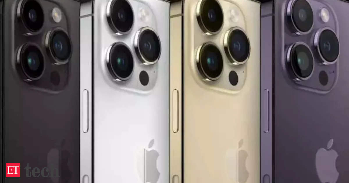
I read that Apple too make less Iphones because Demand is not there.
I mean that could make space for Nintendo to step in?

Not necessarily.

Demand for higher-priced iPhone 14 Pro models is stronger than for the entry-level versions, according to some of the people. In at least one case, an Apple supplier is shifting production capacity from lower-priced iPhones to premium models, they added.
 
0
The article you are reading is an updated version of what I shared on Discord a few weeks ago, so there is much more information than you saw in that archive. This is still just a temporary overview of the hardware of the potential Switch 2, Nintendo's next-generation console that will replace the current Nintendo Switch in the market.

The Switch 2's main chip

The main chip of the console has been designed by NVIDIA, it is unknown which manufacturing node Nintendo and NVIDIA have opted for, at first it was going to be manufactured under TSMC's N7 node, but everything points to the choice being the N6 node. The SoC is completely custom, so it will not be used in any product other than Nintendo's next console and is codenamed T239.

We know this from NVIDIA's leaked documentation a few months ago from the attack on their lapse servers. Thanks to this we were able to know that the T239 is the chip of the Nintendo Switch 2 by being related to the NVN2 API. Remember that NVN is the Nintendo Switch graphics API, so this would be an improved version of the one used in Switch.

Coprocessors

However, despite being derived from the Tegra, which are now automotive-focused, a good part of the coprocessors included for it have been discarded in the process, so the only ones included in the chip, apart from the CPU and GPU are:

The chip can play video in all kinds of formats, including AV1. It actually inherits from the Tegra Orin its NVDEC. Unfortunately, Nintendo has taken away its ability to encode video through NVENC.
The Audio Processor Engine or APE is in charge of audio processing on the Tegra and therefore the music and sound libraries of the games depend on it. So it is obviously a unit that is maintained.
The VIC or Video Integrated Controller is the one that reads the image buffer and transmits it through the video signal to the display. Whether it is the console's own display or an external TV.
The chip contains temperature sensors that act in conjunction with the coprocessor responsible for carrying out the control of the system. This coprocessor is important in Switch 2 and is responsible for handling the following parameters:
The frequency and voltage of the CPU and GPU.
The number of active cores at any given time.
To turn coprocessors on and off when they are not in use.
A final coprocessor is a DMA unit with on-the-fly data compression and decompression for transfer between storage and RAM and vice versa.
Clock frequencies and CPU-to-GPU ratio

In Switch 2 the concept of Dock mode and Undock mode (portable) has completely disappeared, the console has adopted the same concept as NVIDIA's Max-Q/Max-P that AMD would later copy in the form of Smartshift, which went to PS5, and, therefore, we are talking about clock rates being dynamic and not static. The coprocessor in charge of keeping track of the system takes the different values depending on the load level in the game.

If the CPU is on high, then the GPU is set to low.
On the other hand, if the GPU is on high, then the CPU is set to low.
There is a balanced mode where both run at medium speed.
When we are browsing the console menu or in the eShop, the system is designed to use only 2 CPU cores at the lowest supported speed and the GPU with most of its cores disabled except 2 SM and also running at the lowest possible speed. The first CPU core controls the operating system and is isolated from the rest, the second one is in charge of handling the menu environment and when we load a game this environment remains in the background in the system RAM.

The number of GPU SM cores and CPU cores can be disabled when they are not needed. This is not done by the game code, but if a part of the chip is unused, it is immediately de-energized. It is precisely the part in charge of battery life that they have optimized the most, so games do not use 100% of the hardware all the time.

The CPU

The core processor is two full Cortex A78E clusters of four cores each, all with a 2 MB L2 cache per cluster. So we have a total of 8 cores. Nintendo and NVIDIA have not placed any additional support processors in the form of e.g. the A55. The processor also does not support multithreading.

Its power is higher per clock cycle than PS4 and Xbox One CPUs, but it is a far cry from those of the current generation. Moreover, in Switch backwards compatible mode it runs in a limited way at 1020 MHz and using only 4 cores. In contrast, in Switch 2 mode it has 3 clock speeds that depend on the workload at the time.

L3 cache

The Switch 2 SoC has 4 MB of third level cache, which is located before the memory controller and is responsible for making all RAM accesses between CPU and GPU coherent and that these can also pass messages to each other without passing through RAM. This reduces power consumption and communication latency. In backward compatible mode this cache is not used and is completely disabled.

GPU

The graphics processor in Switch 2 was designed with the recently released RTX 30, so its SM cores are exactly the same as you can find in the RTX 30. Actually the internal name of it is GA10B and a trimmed version of the RTX 3050.

I have made a quick diagram so you can get a visual idea of it, which is much easier to understand


Descriptively, the Switch 2 GPU has the following features:

Unlike Switch's TX1 where we only had one GPC, we now have two, so the number of raster triangles per clock cycle has doubled.
The number of GPU cores, SM in NVIDIA slang, is now 12.
Each SM has the same configuration as NVIDIA's RTX 30 and RTX 40.
That is: 64 ALUs in FP32 + 64 ALUs FP32/INT32 switched. This makes 1536 32 bit floating point units.
Twice as many as Xbox One.
50% more than PlayStation 4
3 times more than Steam Deck.
Inside each SM has the corresponding Tensor units to perform the NVN DLSS, a variant of the PC DLSS 2 optimized for the Nintendo Switch 2.
NVN DLSS is only used in dock mode, where the GPU is set to a higher clock speed to trigger the algorithm and scale from 1080p to 4K.
If the connected TV is Full HD then NVN DLSS is not activated.
At the moment, neither Nintendo nor NVIDIA have found a single Switch game that requires the use of DLSS to run at Full HD resolution and 60 FPS.
Unlike the Tegra, each SM has an RT Core for Ray Tracing, which is the same used in the different RTX 30 graphics cards.
We have only 8 ROPS per GPC for a total of 16, so the fill rate has been cut per GPC by half.
The idea is that the impact of the fill rate on system RAM bandwidth is not as large.
Interestingly, the fill rate is the same as Switch.
The clock speed of the entire GPU is 768 MHz in handheld mode and can reach an unknown higher speed in Dock mode if NVN DLSS is enabled.
Switch games when running on the new console run directly in Dock mode.

RAM memory

This is one of the most controversial parts of the new system, as the bandwidth is lower than that of the Steam Deck, since despite also using LPDDR5 memory with a 128-bit bus, its bandwidth is 68 GB/s, due to the fact that it is LPDDR5-4266 instead of LPDDR5-5500. The other difference is that Nintendo's console has 8 GB, of which only 4 GB is used in backwards compatible mode, while Switch 2 games have access to the entire system RAM.

The RAM is not located inside the chip, but in the main circuitry. In order to save space, Nintendo and NVIDIA have done something very similar to what they did with the first Wii and Wii U, and what Apple has also done with its M1 and M2 processors for Mac. Putting everything on top of a common interposer or communication chip to reduce the space occupied by the circuitry.

Other Switch 2 details outside the main SoC

These details are based on leaked documentation, logic and some loose chats with one or another engineer of the project. It should be noted that NVIDIA does not have the complete schematic in order to avoid leaks.

Contrary to what some doomsayers say, the console will continue to have Gamecards as physical distribution of games. The physical storages offered by Nintendo to publishers are the almost the same as with the original Switch, however, with some changes:
Nintendo will no longer offer 1GB, 2GB or 4GB Gamecards. Any game that takes up that much space will be distributed exclusively on the eShop.
Switch 2 Gamecards are 8, 16, 32 and 64 GB.
At the moment, the Switch 2 ones are differentiated by having a gray color that matches the magnesium casing of the main part of the console.
At first glance they would be the same as the Switch, but somewhat wider so that they can not be placed in the normal Switch.
The number of pins is the same.
The transfer clock speed is 100 MHz.
The console can read the Gamecards from the first Switch without problems.
The data on the Switch 2 cards are compressed as standard.
The decompression of that data is carried out by a new coprocessor,
Think of it as a small-scale version of the PS5 and Xbox Series analog units.
Thanks to this, not only the loading times, console startup, but also the installation of games from the eShop have been improved.
As for the screen, for the moment it is unknown what it is, the system supports both IPS and OLED panels.
It is known that it will be HDR at Full HD resolution.
The charging and video transmission connector remains the USB-C Alt-DP.
Its bandwidth is the same as that of the Switch.
Its power supply power is higher, so it can charge the Switch 2's battery in less time.
The space occupied by the system circuitry is smaller than in Switch, while more space has been given to the battery. The battery also has a larger capacity.
The fan now has a slightly larger diameter, plus there is a micro-dotted air outlet on the back of the magnesium alloy case.
At the moment they are testing the circuitry using controllers from the first Switch and the OLED version Dock of the Switch.
They don't know if Nintendo will add any gimmicks to the console at the last minute, as NVIDIA's job is to make sure the available games work with the new hardware.
As a curiosity, the SDK has two NAND Flash memories instead of one.
The first one is Boot0 and corresponds to the original Switch environment.
The second one is Boot1 where there is a Linux distribution where the NVN2 API is being tested.
Inside are included some technical demos based on classic Nintendo games to show the capabilities of the console at a technical level. These are based on classic GameCube and Nintendo64 games.
This is clearly all bullshit, except for a few known things from the Nvidia leak, which seem to be taken secondhand from Famiboards or another source.
 
The article you are reading is an updated version of what I shared on Discord a few weeks ago, so there is much more information than you saw in that archive. This is still just a temporary overview of the hardware of the potential Switch 2, Nintendo's next-generation console that will replace the current Nintendo Switch in the market.

The Switch 2's main chip

The main chip of the console has been designed by NVIDIA, it is unknown which manufacturing node Nintendo and NVIDIA have opted for, at first it was going to be manufactured under TSMC's N7 node, but everything points to the choice being the N6 node. The SoC is completely custom, so it will not be used in any product other than Nintendo's next console and is codenamed T239.

We know this from NVIDIA's leaked documentation a few months ago from the attack on their lapse servers. Thanks to this we were able to know that the T239 is the chip of the Nintendo Switch 2 by being related to the NVN2 API. Remember that NVN is the Nintendo Switch graphics API, so this would be an improved version of the one used in Switch.

Coprocessors

However, despite being derived from the Tegra, which are now automotive-focused, a good part of the coprocessors included for it have been discarded in the process, so the only ones included in the chip, apart from the CPU and GPU are:

The chip can play video in all kinds of formats, including AV1. It actually inherits from the Tegra Orin its NVDEC. Unfortunately, Nintendo has taken away its ability to encode video through NVENC.
The Audio Processor Engine or APE is in charge of audio processing on the Tegra and therefore the music and sound libraries of the games depend on it. So it is obviously a unit that is maintained.
The VIC or Video Integrated Controller is the one that reads the image buffer and transmits it through the video signal to the display. Whether it is the console's own display or an external TV.
The chip contains temperature sensors that act in conjunction with the coprocessor responsible for carrying out the control of the system. This coprocessor is important in Switch 2 and is responsible for handling the following parameters:
The frequency and voltage of the CPU and GPU.
The number of active cores at any given time.
To turn coprocessors on and off when they are not in use.
A final coprocessor is a DMA unit with on-the-fly data compression and decompression for transfer between storage and RAM and vice versa.
Clock frequencies and CPU-to-GPU ratio

In Switch 2 the concept of Dock mode and Undock mode (portable) has completely disappeared, the console has adopted the same concept as NVIDIA's Max-Q/Max-P that AMD would later copy in the form of Smartshift, which went to PS5, and, therefore, we are talking about clock rates being dynamic and not static. The coprocessor in charge of keeping track of the system takes the different values depending on the load level in the game.

If the CPU is on high, then the GPU is set to low.
On the other hand, if the GPU is on high, then the CPU is set to low.
There is a balanced mode where both run at medium speed.
When we are browsing the console menu or in the eShop, the system is designed to use only 2 CPU cores at the lowest supported speed and the GPU with most of its cores disabled except 2 SM and also running at the lowest possible speed. The first CPU core controls the operating system and is isolated from the rest, the second one is in charge of handling the menu environment and when we load a game this environment remains in the background in the system RAM.

The number of GPU SM cores and CPU cores can be disabled when they are not needed. This is not done by the game code, but if a part of the chip is unused, it is immediately de-energized. It is precisely the part in charge of battery life that they have optimized the most, so games do not use 100% of the hardware all the time.

The CPU

The core processor is two full Cortex A78E clusters of four cores each, all with a 2 MB L2 cache per cluster. So we have a total of 8 cores. Nintendo and NVIDIA have not placed any additional support processors in the form of e.g. the A55. The processor also does not support multithreading.

Its power is higher per clock cycle than PS4 and Xbox One CPUs, but it is a far cry from those of the current generation. Moreover, in Switch backwards compatible mode it runs in a limited way at 1020 MHz and using only 4 cores. In contrast, in Switch 2 mode it has 3 clock speeds that depend on the workload at the time.

L3 cache

The Switch 2 SoC has 4 MB of third level cache, which is located before the memory controller and is responsible for making all RAM accesses between CPU and GPU coherent and that these can also pass messages to each other without passing through RAM. This reduces power consumption and communication latency. In backward compatible mode this cache is not used and is completely disabled.

GPU

The graphics processor in Switch 2 was designed with the recently released RTX 30, so its SM cores are exactly the same as you can find in the RTX 30. Actually the internal name of it is GA10B and a trimmed version of the RTX 3050.

I have made a quick diagram so you can get a visual idea of it, which is much easier to understand


Descriptively, the Switch 2 GPU has the following features:

Unlike Switch's TX1 where we only had one GPC, we now have two, so the number of raster triangles per clock cycle has doubled.
The number of GPU cores, SM in NVIDIA slang, is now 12.
Each SM has the same configuration as NVIDIA's RTX 30 and RTX 40.
That is: 64 ALUs in FP32 + 64 ALUs FP32/INT32 switched. This makes 1536 32 bit floating point units.
Twice as many as Xbox One.
50% more than PlayStation 4
3 times more than Steam Deck.
Inside each SM has the corresponding Tensor units to perform the NVN DLSS, a variant of the PC DLSS 2 optimized for the Nintendo Switch 2.
NVN DLSS is only used in dock mode, where the GPU is set to a higher clock speed to trigger the algorithm and scale from 1080p to 4K.
If the connected TV is Full HD then NVN DLSS is not activated.
At the moment, neither Nintendo nor NVIDIA have found a single Switch game that requires the use of DLSS to run at Full HD resolution and 60 FPS.
Unlike the Tegra, each SM has an RT Core for Ray Tracing, which is the same used in the different RTX 30 graphics cards.
We have only 8 ROPS per GPC for a total of 16, so the fill rate has been cut per GPC by half.
The idea is that the impact of the fill rate on system RAM bandwidth is not as large.
Interestingly, the fill rate is the same as Switch.
The clock speed of the entire GPU is 768 MHz in handheld mode and can reach an unknown higher speed in Dock mode if NVN DLSS is enabled.
Switch games when running on the new console run directly in Dock mode.

RAM memory

This is one of the most controversial parts of the new system, as the bandwidth is lower than that of the Steam Deck, since despite also using LPDDR5 memory with a 128-bit bus, its bandwidth is 68 GB/s, due to the fact that it is LPDDR5-4266 instead of LPDDR5-5500. The other difference is that Nintendo's console has 8 GB, of which only 4 GB is used in backwards compatible mode, while Switch 2 games have access to the entire system RAM.

The RAM is not located inside the chip, but in the main circuitry. In order to save space, Nintendo and NVIDIA have done something very similar to what they did with the first Wii and Wii U, and what Apple has also done with its M1 and M2 processors for Mac. Putting everything on top of a common interposer or communication chip to reduce the space occupied by the circuitry.

Other Switch 2 details outside the main SoC

These details are based on leaked documentation, logic and some loose chats with one or another engineer of the project. It should be noted that NVIDIA does not have the complete schematic in order to avoid leaks.

Contrary to what some doomsayers say, the console will continue to have Gamecards as physical distribution of games. The physical storages offered by Nintendo to publishers are the almost the same as with the original Switch, however, with some changes:
Nintendo will no longer offer 1GB, 2GB or 4GB Gamecards. Any game that takes up that much space will be distributed exclusively on the eShop.
Switch 2 Gamecards are 8, 16, 32 and 64 GB.
At the moment, the Switch 2 ones are differentiated by having a gray color that matches the magnesium casing of the main part of the console.
At first glance they would be the same as the Switch, but somewhat wider so that they can not be placed in the normal Switch.
The number of pins is the same.
The transfer clock speed is 100 MHz.
The console can read the Gamecards from the first Switch without problems.
The data on the Switch 2 cards are compressed as standard.
The decompression of that data is carried out by a new coprocessor,
Think of it as a small-scale version of the PS5 and Xbox Series analog units.
Thanks to this, not only the loading times, console startup, but also the installation of games from the eShop have been improved.
As for the screen, for the moment it is unknown what it is, the system supports both IPS and OLED panels.
It is known that it will be HDR at Full HD resolution.
The charging and video transmission connector remains the USB-C Alt-DP.
Its bandwidth is the same as that of the Switch.
Its power supply power is higher, so it can charge the Switch 2's battery in less time.
The space occupied by the system circuitry is smaller than in Switch, while more space has been given to the battery. The battery also has a larger capacity.
The fan now has a slightly larger diameter, plus there is a micro-dotted air outlet on the back of the magnesium alloy case.
At the moment they are testing the circuitry using controllers from the first Switch and the OLED version Dock of the Switch.
They don't know if Nintendo will add any gimmicks to the console at the last minute, as NVIDIA's job is to make sure the available games work with the new hardware.
As a curiosity, the SDK has two NAND Flash memories instead of one.
The first one is Boot0 and corresponds to the original Switch environment.
The second one is Boot1 where there is a Linux distribution where the NVN2 API is being tested.
Inside are included some technical demos based on classic Nintendo games to show the capabilities of the console at a technical level. These are based on classic GameCube and Nintendo64 games.

This all sounds pretty good if it's indeed real. Probably inline with my personal speculation. A bit low on the ram though but we'll have to wait and see if that ends up being a bottleneck or not down the road with some of these "impossible ports". now the real question is, any chance for this to actually being real? It's pretty well written but the CPU clusters seem to be different then those Linux logs suggested as mentioned above so I don't know.
 
Nice to meet you.
I was surfing the net and found the following information. What do you think?
This is wild. What's the source? The user says they've shared some stuff on discord before, presumably going into their source some, but they're not saying anything here. Do you know anything about this person?

My spanish is awful, so I may be misunderstanding some of the finer details. But I don't buy it. The user makes one claim we know is wrong - A78E, 2 quad core clusters. The A78E doesn't exist, and the linux drops say an 8core cluster. However, the implication of the rest of the post is that they're working from insiders with dev kits, which may have been based on Orin, so it doesn't totally rule them out. But it's not the only bad smell.

Other claims in the hidey tag

Hidden content is only available for registered users. Sharing it outside of Famiboards is subject to moderation.


And that's it. There is enough to not trust here, combined with stuff we already knew that I have trouble taking it seriously. A few of the claims are intriguing, other's are disappointing. The best case scenario for this leaker's truthfulness is that they have multiple sources over a wide time period and have combined everything they know, even when inconsistent.
 
Sure the new version would be running at a higher framerate and resolution, but I think they would need to do a bit more in order for it to seems like a worthwhile upgrade for many consumers.
I tend to think they'll put in the effort ... at least for zelda
 
0
This is wild. What's the source? The user says they've shared some stuff on discord before, presumably going into their source some, but they're not saying anything here. Do you know anything about this person?

My spanish is awful, so I may be misunderstanding some of the finer details. But I don't buy it. The user makes one claim we know is wrong - A78E, 2 quad core clusters. The A78E doesn't exist, and the linux drops say an 8core cluster. However, the implication of the rest of the post is that they're working from insiders with dev kits, which may have been based on Orin, so it doesn't totally rule them out. But it's not the only bad smell.

Other claims in the hidey tag

* Hidden text: cannot be quoted. *


And that's it. There is enough to not trust here, combined with stuff we already knew that I have trouble taking it seriously. A few of the claims are intriguing, other's are disappointing. The best case scenario for this leaker's truthfulness is that they have multiple sources over a wide time period and have combined everything they know, even when inconsistent.
I will say this. This whole document implies a slightly different design than the device we often talk about here. It can't be a "PS4 in handheld mode + DLSS" because this design has no DLSS in handheld mode. Instead, it's a design that looks a little bit more like a steamdeck, a 1080p targeting device that "happens" to dock, and DLSS despite it's deeper software integration, to the user acts like one of those magic upscaling dongles (just with decent quality output).

In other words, and I hate to say this, because again, this post gives me Bad Smells BUT - if you had a 2.0 level SOC but wanted to build a 1.5 level device out of it - make a Pro in other words - this would be the approach you could take. Use your new SOC to just drag everything in your old library up to 1080p, use some software tricks to force old games to run their highest quality mode no matter what, and then 4k is just a "magic feature"

The dynamic clocks sets the stage for you to come along later and do an actual Switch 2 on the same (possibly die shrunk) architecture, with few back compat hurdles in your way
 
This is wild. What's the source? The user says they've shared some stuff on discord before, presumably going into their source some, but they're not saying anything here. Do you know anything about this person?

My spanish is awful, so I may be misunderstanding some of the finer details. But I don't buy it. The user makes one claim we know is wrong - A78E, 2 quad core clusters. The A78E doesn't exist, and the linux drops say an 8core cluster. However, the implication of the rest of the post is that they're working from insiders with dev kits, which may have been based on Orin, so it doesn't totally rule them out. But it's not the only bad smell.

Other claims in the hidey tag

* Hidden text: cannot be quoted. *


And that's it. There is enough to not trust here, combined with stuff we already knew that I have trouble taking it seriously. A few of the claims are intriguing, other's are disappointing. The best case scenario for this leaker's truthfulness is that they have multiple sources over a wide time period and have combined everything they know, even when inconsistent.
They claimed Nintendo and Nvidia have yet to get an og switch game to 1080/60 on this new hardware, not 4K. Implication is that if you only have a 1080 panel there would be no need to activate the DLSS profile.

I’m a laymen here but I know there is supposed to be some huge benefits with placing the ram inside the soc package like apple has done it. I believe it makes it so the GPU and CPU have access simultaneously and there is less reloading of data or something. Not sure how that would effect gaming but there might be something there to consider.

Really interesting article. Could be a bunch of make believe but wow they are getting very specific about certain things that they don’t need to be specific about. Very interesting, OP!
 
The article you are reading is an updated version of what I shared on Discord a few weeks ago, so there is much more information than you saw in that archive. This is still just a temporary overview of the hardware of the potential Switch 2, Nintendo's next-generation console that will replace the current Nintendo Switch in the market.

The Switch 2's main chip

The main chip of the console has been designed by NVIDIA, it is unknown which manufacturing node Nintendo and NVIDIA have opted for, at first it was going to be manufactured under TSMC's N7 node, but everything points to the choice being the N6 node. The SoC is completely custom, so it will not be used in any product other than Nintendo's next console and is codenamed T239.

We know this from NVIDIA's leaked documentation a few months ago from the attack on their lapse servers. Thanks to this we were able to know that the T239 is the chip of the Nintendo Switch 2 by being related to the NVN2 API. Remember that NVN is the Nintendo Switch graphics API, so this would be an improved version of the one used in Switch.

Coprocessors

However, despite being derived from the Tegra, which are now automotive-focused, a good part of the coprocessors included for it have been discarded in the process, so the only ones included in the chip, apart from the CPU and GPU are:

The chip can play video in all kinds of formats, including AV1. It actually inherits from the Tegra Orin its NVDEC. Unfortunately, Nintendo has taken away its ability to encode video through NVENC.
The Audio Processor Engine or APE is in charge of audio processing on the Tegra and therefore the music and sound libraries of the games depend on it. So it is obviously a unit that is maintained.
The VIC or Video Integrated Controller is the one that reads the image buffer and transmits it through the video signal to the display. Whether it is the console's own display or an external TV.
The chip contains temperature sensors that act in conjunction with the coprocessor responsible for carrying out the control of the system. This coprocessor is important in Switch 2 and is responsible for handling the following parameters:
The frequency and voltage of the CPU and GPU.
The number of active cores at any given time.
To turn coprocessors on and off when they are not in use.
A final coprocessor is a DMA unit with on-the-fly data compression and decompression for transfer between storage and RAM and vice versa.
Clock frequencies and CPU-to-GPU ratio

In Switch 2 the concept of Dock mode and Undock mode (portable) has completely disappeared, the console has adopted the same concept as NVIDIA's Max-Q/Max-P that AMD would later copy in the form of Smartshift, which went to PS5, and, therefore, we are talking about clock rates being dynamic and not static. The coprocessor in charge of keeping track of the system takes the different values depending on the load level in the game.

If the CPU is on high, then the GPU is set to low.
On the other hand, if the GPU is on high, then the CPU is set to low.
There is a balanced mode where both run at medium speed.
When we are browsing the console menu or in the eShop, the system is designed to use only 2 CPU cores at the lowest supported speed and the GPU with most of its cores disabled except 2 SM and also running at the lowest possible speed. The first CPU core controls the operating system and is isolated from the rest, the second one is in charge of handling the menu environment and when we load a game this environment remains in the background in the system RAM.

The number of GPU SM cores and CPU cores can be disabled when they are not needed. This is not done by the game code, but if a part of the chip is unused, it is immediately de-energized. It is precisely the part in charge of battery life that they have optimized the most, so games do not use 100% of the hardware all the time.

The CPU

The core processor is two full Cortex A78E clusters of four cores each, all with a 2 MB L2 cache per cluster. So we have a total of 8 cores. Nintendo and NVIDIA have not placed any additional support processors in the form of e.g. the A55. The processor also does not support multithreading.

Its power is higher per clock cycle than PS4 and Xbox One CPUs, but it is a far cry from those of the current generation. Moreover, in Switch backwards compatible mode it runs in a limited way at 1020 MHz and using only 4 cores. In contrast, in Switch 2 mode it has 3 clock speeds that depend on the workload at the time.

L3 cache

The Switch 2 SoC has 4 MB of third level cache, which is located before the memory controller and is responsible for making all RAM accesses between CPU and GPU coherent and that these can also pass messages to each other without passing through RAM. This reduces power consumption and communication latency. In backward compatible mode this cache is not used and is completely disabled.

GPU

The graphics processor in Switch 2 was designed with the recently released RTX 30, so its SM cores are exactly the same as you can find in the RTX 30. Actually the internal name of it is GA10B and a trimmed version of the RTX 3050.

I have made a quick diagram so you can get a visual idea of it, which is much easier to understand


Descriptively, the Switch 2 GPU has the following features:

Unlike Switch's TX1 where we only had one GPC, we now have two, so the number of raster triangles per clock cycle has doubled.
The number of GPU cores, SM in NVIDIA slang, is now 12.
Each SM has the same configuration as NVIDIA's RTX 30 and RTX 40.
That is: 64 ALUs in FP32 + 64 ALUs FP32/INT32 switched. This makes 1536 32 bit floating point units.
Twice as many as Xbox One.
50% more than PlayStation 4
3 times more than Steam Deck.
Inside each SM has the corresponding Tensor units to perform the NVN DLSS, a variant of the PC DLSS 2 optimized for the Nintendo Switch 2.
NVN DLSS is only used in dock mode, where the GPU is set to a higher clock speed to trigger the algorithm and scale from 1080p to 4K.
If the connected TV is Full HD then NVN DLSS is not activated.
At the moment, neither Nintendo nor NVIDIA have found a single Switch game that requires the use of DLSS to run at Full HD resolution and 60 FPS.
Unlike the Tegra, each SM has an RT Core for Ray Tracing, which is the same used in the different RTX 30 graphics cards.
We have only 8 ROPS per GPC for a total of 16, so the fill rate has been cut per GPC by half.
The idea is that the impact of the fill rate on system RAM bandwidth is not as large.
Interestingly, the fill rate is the same as Switch.
The clock speed of the entire GPU is 768 MHz in handheld mode and can reach an unknown higher speed in Dock mode if NVN DLSS is enabled.
Switch games when running on the new console run directly in Dock mode.

RAM memory

This is one of the most controversial parts of the new system, as the bandwidth is lower than that of the Steam Deck, since despite also using LPDDR5 memory with a 128-bit bus, its bandwidth is 68 GB/s, due to the fact that it is LPDDR5-4266 instead of LPDDR5-5500. The other difference is that Nintendo's console has 8 GB, of which only 4 GB is used in backwards compatible mode, while Switch 2 games have access to the entire system RAM.

The RAM is not located inside the chip, but in the main circuitry. In order to save space, Nintendo and NVIDIA have done something very similar to what they did with the first Wii and Wii U, and what Apple has also done with its M1 and M2 processors for Mac. Putting everything on top of a common interposer or communication chip to reduce the space occupied by the circuitry.

Other Switch 2 details outside the main SoC

These details are based on leaked documentation, logic and some loose chats with one or another engineer of the project. It should be noted that NVIDIA does not have the complete schematic in order to avoid leaks.

Contrary to what some doomsayers say, the console will continue to have Gamecards as physical distribution of games. The physical storages offered by Nintendo to publishers are the almost the same as with the original Switch, however, with some changes:
Nintendo will no longer offer 1GB, 2GB or 4GB Gamecards. Any game that takes up that much space will be distributed exclusively on the eShop.
Switch 2 Gamecards are 8, 16, 32 and 64 GB.
At the moment, the Switch 2 ones are differentiated by having a gray color that matches the magnesium casing of the main part of the console.
At first glance they would be the same as the Switch, but somewhat wider so that they can not be placed in the normal Switch.
The number of pins is the same.
The transfer clock speed is 100 MHz.
The console can read the Gamecards from the first Switch without problems.
The data on the Switch 2 cards are compressed as standard.
The decompression of that data is carried out by a new coprocessor,
Think of it as a small-scale version of the PS5 and Xbox Series analog units.
Thanks to this, not only the loading times, console startup, but also the installation of games from the eShop have been improved.
As for the screen, for the moment it is unknown what it is, the system supports both IPS and OLED panels.
It is known that it will be HDR at Full HD resolution.
The charging and video transmission connector remains the USB-C Alt-DP.
Its bandwidth is the same as that of the Switch.
Its power supply power is higher, so it can charge the Switch 2's battery in less time.
The space occupied by the system circuitry is smaller than in Switch, while more space has been given to the battery. The battery also has a larger capacity.
The fan now has a slightly larger diameter, plus there is a micro-dotted air outlet on the back of the magnesium alloy case.
At the moment they are testing the circuitry using controllers from the first Switch and the OLED version Dock of the Switch.
They don't know if Nintendo will add any gimmicks to the console at the last minute, as NVIDIA's job is to make sure the available games work with the new hardware.
As a curiosity, the SDK has two NAND Flash memories instead of one.
The first one is Boot0 and corresponds to the original Switch environment.
The second one is Boot1 where there is a Linux distribution where the NVN2 API is being tested.
Inside are included some technical demos based on classic Nintendo games to show the capabilities of the console at a technical level. These are based on classic GameCube and Nintendo64 games.

Says the hardware doesn’t distinguish between docked and undocked but then goes on to say DLSS only works in docked.
 
I read that Apple too make less Iphones because Demand is not there.
I mean that could make space for Nintendo to step in?

Every single year there is articles like this – Apple is frantically scaling back on orders due to a lack of demand. And somehow, the iPhone seems to only get more popular.

I wouldn’t read too much into this, especially since by all accounts the Pro models seem to be capturing an even larger share of iPhone sales than before. Which isn’t too surprising, since for the first time going Pro is required to get the latest generation SoC.
 
Says the hardware doesn’t distinguish between docked and undocked but then goes on to say DLSS only works in docked.
I don’t think it’s genuine, but in this situation I would imagine it doesn’t differentiate between docked and undocked, it differentiates based on output resolution. Borne out by the fact that it says DLSS does not engage for 1080p docked output.
 
@oldpuck Although the rumour doesn't look like it's worth putting any stock in, the mention of compression/decompression does raise one thing that's been in the back of my mind: the FDE block on T239. It's mentioned here among other places, and seems to only be on T239, not T234. I haven't seen anything to indicate what it is, though, and I'm very curious as it seems to have been added specifically for the new Switch.

My first instinct when I see FDE was full disk encryption, but that doesn't make much sense for a dedicated block, which leads me to try a game of guess-the-acronym. Do you have any idea of what it is? My only plausible guess so far is that it's a decompression engine of some kind, ie Fast Decompression Engine, or something like that. This would make sense to include as a block on T239 but not T234, as we know it can be a bottleneck on games consoles. Still very much just a random guess, though.

Great post, thank you for taking what I was alluding to as a possibility and conducting a pretty thorough analysis, always enjoy reading your posts.

One other factor to consider, especially when it comes to the higher R and D costs is that the upfront additional cost may completely negate the need for a future die shrink.

I don't think Nintendo would clock a 4N Drake chip that much higher than a 6N one and would bank the extra battery life as a benefit. My reasoning being is that beyond a certain point any extra raw TFLOP gains are going to be negated by memory bandwidth constraints. Therefore the extra R and D now means a saving in having to shrink the chip later.

Not to say that RE-releasing a die shrunk switch is a bad thing. I'm sure there would have been original switch owners who upgraded for extra battery life and thus introduced new people to the infrastructure through the second hand market. It also acts as a kind of soft relaunch, but there are other things Nintendo can do to reinvigorate switch sales.

This is why my stance is now that 4N seems more likely that Samsung 8nm given the potential enormity of Drake on 8nm.

Yeah, I do think if the plan was to spend the R&D to fab it on 7nm, then in two years spend a bunch more R&D to shrink it to 5nm, why not just build it on 5nm in the first place? I'd agree that I don't expect much higher clocks on 5nm than 7nm/6nm, and potentially they could use the same chip in a Drake Lite without having to do a die shrink. They'd have to wait for costs to come down a bit to make a cheaper portable-only model viable, but if they plan to release such a model, it makes more sense to me to just build the chip on 5nm in the first place.

Another thing to add to this is Nvidia does have AI fab tech that allows them to shrink dies faster and we did hear about "Dane" code name for T239, that happened to be magically word blocked in the Nvidia hack, it's possible they did a die shrink whenever brainchild mentioned some power issues in early 2021.

The problem I have with the idea that Nintendo was initially planning on using a worse node a shrunk it is that both they and Nvidia would have known exactly what to expect from Samsung's 8nm and TSMC's 7nm process when they started development. They wouldn't have started off with the idea that 12 SMs would be no problem on a portable device on 8nm and then only realised later that it consumes way too much power. Ditto with 7nm, which would have been a known quantity by that stage. The only nodes that would have surprised them would be Samsung's 7nm and smaller processes. These are definitely performing worse than expected (ask Qualcomm), but I'd be surprised if they were planning to use one of these nodes in the first place, and if they had to switch from let's say Samsung 5nm to TSMC 5nm, then I would imagine that would result in a significant delay to the hardware of as much as a year, which doesn't seem to have happened.

Also, do you have a source for the Nvidia AI fab tech? I saw an article a while back on how they used AI for the layout of a single block on Hopper, but it seemed very much like early steps, and not something ready for laying out an entire SoC.
 
Last edited:
They claimed Nintendo and Nvidia have yet to get an og switch game to 1080/60 on this new hardware, not 4K. Implication is that if you only have a 1080 panel there would be no need to activate the DLSS profile.
I believe what they were saying is that they've not found an OG Switch game they can't push to 1080p. Which is odd, considering that they state definitively that the CPU runs 1GHz during backwards compat, meaning that games running in BC mode should not see a perf boost, but I'm giving them the benefit of the doubt that they mean games patched to run on Drake.

The DLSS profile in docked mode only makes sense not just if you have a 1080p panel, but also if you're running identical clocks in both handheld and docked mode. Which... yeah, I can see it. You spend the extra power draw in docked mode only if you need to activate tensor cores, plus some light overclocking to get the perf needed for upscaling.

But games will need to be built against the DLSS api, meaning they're going to be sending the data to the GPU regardless of mode, just ignoring it in handheld. It seems like there is plenty of opportunity to take games that can't hit 1080p and let them run in 720p of lower and DLSS them up, even in handheld mode. Plenty of "impossible ports" struggled to hit max res on the Switch, it seems the next gen impossible ports - Elden Ring, for example - would be in the same boat, and benefit from DLSS period.

I’m a laymen here but I know there is supposed to be some huge benefits with placing the ram inside the soc package like apple has done it. I believe it makes it so the GPU and CPU have access simultaneously and there is less reloading of data or something. Not sure how that would effect gaming but there might be something there to consider.
Apple has done both, I believe. One makes the SOC cheaper to make and makes it easier to utilize third party RAM manufacturing, the other makes smaller, faster, more effecient chips.

Really interesting article. Could be a bunch of make believe but wow they are getting very specific about certain things that they don’t need to be specific about. Very interesting, OP!
 
0
I think one of the things that really stood out in the spanish article, outside of the 2*4 cluster CPU layout, is the 768mhz portable GPU clock.

Seems a bit steep for something that needs to run that in a sustained manner.
 
0
- 2 A78E (?) clusters, 2 MB of L2 cache per cluster, 4 MB of shared L3 cache
Cute. To be clear for the readers, since the A75/introduction of DynamIQ, L2 cache is private to each core and L3 is shared within a cluster. For a chunk of cache shared across all the clusters, it'd be a fourth level, or what Orin calls System Cache.
-NVENC supposedly getting ditched?
Not happening. As long as you have the ability to record video clips and Nintendo remotely gives a damn about efficiency (and we know they very well do), NVENC's staying around.

So anyway, on a different subject (or rather, return to node talk):
Anybody know if the N5 fab in Arizona is for government chips only or for N5 clients in general? One of the... secondary or tertiary amusing aspects of a theoretical Drake-based soc being on 4N is the possibility of it being MADE IN AMERICA. Although that fab isn't expected to start production until 2024.
 

Yes! This is the article I read on the matter and then couldn't find it again. Its fascinating stuff.

Reinforcement learning is an area I have a keen interest in and can't wait to experiment with in the workplace. It's one area where being a gamer helps with applying data science principles as if you can frame problems like playing a game and trying to get the high score you have a potential application of reinforcement learning.
 
0
- 2 A78E (?) clusters, 2 MB of L2 cache per cluster, 4 MB of shared L3 cache
Cute. To be clear for the readers, since the A75/introduction of DynamIQ, L2 cache is private to each core and L3 is shared within a cluster. For a chunk of cache shared across all the clusters, it'd be a fourth level, or what Orin calls System Cache.
-NVENC supposedly getting ditched?

NVENC isn't getting ditched, it's clearly in the Linux drivers
@oldpuck Although the rumour doesn't look like it's worth putting any stock in, the mention of compression/decompression does raise one thing that's been in the back of my mind: the FDE block on T239. It's mentioned here among other places, and seems to only be on T239, not T234. I haven't seen anything to indicate what it is, though, and I'm very curious as it seems to have been added specifically for the new Switch.

My first instinct when I see FDE was full disk encryption, but that doesn't make much sense for a dedicated block, which leads me to try a game of guess-the-acronym. Do you have any idea of what it is? My only plausible guess so far is that it's a decompression engine of some kind, ie Fast Decompression Engine, or something like that. This would make sense to include as a block on T234 but not T239, as we know it can be a bottleneck on games consoles. Still very much just a random guess, though.
Just guesses. FDE makes me think "Falcon". I don't know if the TX1 had dedicated decompression blocks, but I know Xbox and Playstation have both used them in the past (though I believe Microsoft was trying to get the GPU to do it, to cut down on the number of fixed function blocks they have)
 
Just guesses. FDE makes me think "Falcon". I don't know if the TX1 had dedicated decompression blocks, but I know Xbox and Playstation have both used them in the past (though I believe Microsoft was trying to get the GPU to do it, to cut down on the number of fixed function blocks they have)
Nintendo also had it with the GameCube I believe, a decompression block.


That said, you mentioned Falcon before but I don’t remember in what context, can you refresh it?
 
Oh yea, is the LPDDR5-4266 claim saying that 4266 MT/s is in software/profile preset or in hardware? The former's possible, the latter doesn't exist. (slowest LPDDR5 is capable of 5500 MT/s; 4266 MT/s is pointless because that's 4X speed, and 4X is still being produced)
 
Whatever FDE is, the definition for it is in both T234 and T239 in the leaked driver files.

Edit: Also T232 (which is Atlan or Thor or something).
 
Last edited:
Oh yea, is the LPDDR5-4266 claim saying that 4266 MT/s is in software/profile preset or in hardware? The former's possible, the latter doesn't exist. (slowest LPDDR5 is capable of 5500 MT/s; 4266 MT/s is pointless because that's 4X speed, and 4X is still being produced)
Pretty sure they pulled that one from the Orin nano specs that were announced recently. Maybe via this thread, who knows.
 
Nintendo also had it with the GameCube I believe, a decompression block.


That said, you mentioned Falcon before but I don’t remember in what context, can you refresh it?
Nvidia Falcon is the FAst Logic CONtroller, a chip designed by NVidia for various control systems. It's used in the Tegra Security Module in the original switch - and was one of the vectors for the Switch getting jailbroken. Mariko removed the TSEC.

Since then, Nvidia has dropped the old Falcon design and moved to a new one based on RISC V called "Peregrine." Long term I think they want to drop Falcon compatibility for Peregrine, but for now, it's still backwards compatible.

Both T234 and T239 have a TSEC built on the new Peregrine Falcon[1][2]. But t239 has some batch of Falcon overrides that aren't shared [3] which stick out as odd, but could be simply an attempt to keep T239 data out of the main repo except when absolutely necessary.

 
0

Thanks, I hadn't read that one, very interesting.

NVENC isn't getting ditched, it's clearly in the Linux drivers

Just guesses. FDE makes me think "Falcon". I don't know if the TX1 had dedicated decompression blocks, but I know Xbox and Playstation have both used them in the past (though I believe Microsoft was trying to get the GPU to do it, to cut down on the number of fixed function blocks they have)

I don't think any of the Tegra chips have had dedicated decompression blocks thus far. Or at least general-purpose decompression. There are obviously texture decompression blocks on the GPU and NVDEC is performing decompression as part of the decoding, but not a general "take this file encoded in DEFLATE/LZ78/Zstd/whatever and give me the uncompressed version" block. I'm actually a bit surprised that previous Xbox/Playstation consoles would have included them. I'm aware of the PS5's dedicated hardware for this, but I assumed it just wouldn't have been as big a priority when data speeds were limited by spinning disks of one variety or another.

There is one Nvidia product with a general-purpose decompression block; the BlueField 3 DPU. "Decompression engine" is listed under the hardware accelerators on the spec sheet, although I can't find any more details on it. I'm sure it would be massive overkill to adapt for use in a device like the Switch, though. Bandwidth capabilities are probably an order of magnitude or two more than Switch requires, not to mention that it would likely support a variety of different compression algorithms. Nintendo could get by with support for just one compression algorithm and probably a far simpler design than would be required for a DPU.

Nintendo also had it with the GameCube I believe, a decompression block.


That said, you mentioned Falcon before but I don’t remember in what context, can you refresh it?

The GameCube was novel in that it had hardware texture decompression (S3TC, I believe). I don't think it had a general purpose decompression block, though.

Whatever FDE is, the definition for it is in both T234 and T239 in the leaked driver files.

Thanks. I'm curious why it's not included for T234 in Linux in that case. They seem to have Linux support for it on T239 in some form or another, but no mention of it for T239 from what I can find.
 
0
The article you are reading is an updated version of what I shared on Discord a few weeks ago, so there is much more information than you saw in that archive. This is still just a temporary overview of the hardware of the potential Switch 2, Nintendo's next-generation console that will replace the current Nintendo Switch in the market.

The Switch 2's main chip

The main chip of the console has been designed by NVIDIA, it is unknown which manufacturing node Nintendo and NVIDIA have opted for, at first it was going to be manufactured under TSMC's N7 node, but everything points to the choice being the N6 node. The SoC is completely custom, so it will not be used in any product other than Nintendo's next console and is codenamed T239.

We know this from NVIDIA's leaked documentation a few months ago from the attack on their lapse servers. Thanks to this we were able to know that the T239 is the chip of the Nintendo Switch 2 by being related to the NVN2 API. Remember that NVN is the Nintendo Switch graphics API, so this would be an improved version of the one used in Switch.

Coprocessors

However, despite being derived from the Tegra, which are now automotive-focused, a good part of the coprocessors included for it have been discarded in the process, so the only ones included in the chip, apart from the CPU and GPU are:

The chip can play video in all kinds of formats, including AV1. It actually inherits from the Tegra Orin its NVDEC. Unfortunately, Nintendo has taken away its ability to encode video through NVENC.
The Audio Processor Engine or APE is in charge of audio processing on the Tegra and therefore the music and sound libraries of the games depend on it. So it is obviously a unit that is maintained.
The VIC or Video Integrated Controller is the one that reads the image buffer and transmits it through the video signal to the display. Whether it is the console's own display or an external TV.
The chip contains temperature sensors that act in conjunction with the coprocessor responsible for carrying out the control of the system. This coprocessor is important in Switch 2 and is responsible for handling the following parameters:
The frequency and voltage of the CPU and GPU.
The number of active cores at any given time.
To turn coprocessors on and off when they are not in use.
A final coprocessor is a DMA unit with on-the-fly data compression and decompression for transfer between storage and RAM and vice versa.
Clock frequencies and CPU-to-GPU ratio

In Switch 2 the concept of Dock mode and Undock mode (portable) has completely disappeared, the console has adopted the same concept as NVIDIA's Max-Q/Max-P that AMD would later copy in the form of Smartshift, which went to PS5, and, therefore, we are talking about clock rates being dynamic and not static. The coprocessor in charge of keeping track of the system takes the different values depending on the load level in the game.

If the CPU is on high, then the GPU is set to low.
On the other hand, if the GPU is on high, then the CPU is set to low.
There is a balanced mode where both run at medium speed.
When we are browsing the console menu or in the eShop, the system is designed to use only 2 CPU cores at the lowest supported speed and the GPU with most of its cores disabled except 2 SM and also running at the lowest possible speed. The first CPU core controls the operating system and is isolated from the rest, the second one is in charge of handling the menu environment and when we load a game this environment remains in the background in the system RAM.

The number of GPU SM cores and CPU cores can be disabled when they are not needed. This is not done by the game code, but if a part of the chip is unused, it is immediately de-energized. It is precisely the part in charge of battery life that they have optimized the most, so games do not use 100% of the hardware all the time.

The CPU

The core processor is two full Cortex A78E clusters of four cores each, all with a 2 MB L2 cache per cluster. So we have a total of 8 cores. Nintendo and NVIDIA have not placed any additional support processors in the form of e.g. the A55. The processor also does not support multithreading.

Its power is higher per clock cycle than PS4 and Xbox One CPUs, but it is a far cry from those of the current generation. Moreover, in Switch backwards compatible mode it runs in a limited way at 1020 MHz and using only 4 cores. In contrast, in Switch 2 mode it has 3 clock speeds that depend on the workload at the time.

L3 cache

The Switch 2 SoC has 4 MB of third level cache, which is located before the memory controller and is responsible for making all RAM accesses between CPU and GPU coherent and that these can also pass messages to each other without passing through RAM. This reduces power consumption and communication latency. In backward compatible mode this cache is not used and is completely disabled.

GPU

The graphics processor in Switch 2 was designed with the recently released RTX 30, so its SM cores are exactly the same as you can find in the RTX 30. Actually the internal name of it is GA10B and a trimmed version of the RTX 3050.

I have made a quick diagram so you can get a visual idea of it, which is much easier to understand


Descriptively, the Switch 2 GPU has the following features:

Unlike Switch's TX1 where we only had one GPC, we now have two, so the number of raster triangles per clock cycle has doubled.
The number of GPU cores, SM in NVIDIA slang, is now 12.
Each SM has the same configuration as NVIDIA's RTX 30 and RTX 40.
That is: 64 ALUs in FP32 + 64 ALUs FP32/INT32 switched. This makes 1536 32 bit floating point units.
Twice as many as Xbox One.
50% more than PlayStation 4
3 times more than Steam Deck.
Inside each SM has the corresponding Tensor units to perform the NVN DLSS, a variant of the PC DLSS 2 optimized for the Nintendo Switch 2.
NVN DLSS is only used in dock mode, where the GPU is set to a higher clock speed to trigger the algorithm and scale from 1080p to 4K.
If the connected TV is Full HD then NVN DLSS is not activated.
At the moment, neither Nintendo nor NVIDIA have found a single Switch game that requires the use of DLSS to run at Full HD resolution and 60 FPS.
Unlike the Tegra, each SM has an RT Core for Ray Tracing, which is the same used in the different RTX 30 graphics cards.
We have only 8 ROPS per GPC for a total of 16, so the fill rate has been cut per GPC by half.
The idea is that the impact of the fill rate on system RAM bandwidth is not as large.
Interestingly, the fill rate is the same as Switch.
The clock speed of the entire GPU is 768 MHz in handheld mode and can reach an unknown higher speed in Dock mode if NVN DLSS is enabled.
Switch games when running on the new console run directly in Dock mode.

RAM memory

This is one of the most controversial parts of the new system, as the bandwidth is lower than that of the Steam Deck, since despite also using LPDDR5 memory with a 128-bit bus, its bandwidth is 68 GB/s, due to the fact that it is LPDDR5-4266 instead of LPDDR5-5500. The other difference is that Nintendo's console has 8 GB, of which only 4 GB is used in backwards compatible mode, while Switch 2 games have access to the entire system RAM.

The RAM is not located inside the chip, but in the main circuitry. In order to save space, Nintendo and NVIDIA have done something very similar to what they did with the first Wii and Wii U, and what Apple has also done with its M1 and M2 processors for Mac. Putting everything on top of a common interposer or communication chip to reduce the space occupied by the circuitry.

Other Switch 2 details outside the main SoC

These details are based on leaked documentation, logic and some loose chats with one or another engineer of the project. It should be noted that NVIDIA does not have the complete schematic in order to avoid leaks.

Contrary to what some doomsayers say, the console will continue to have Gamecards as physical distribution of games. The physical storages offered by Nintendo to publishers are the almost the same as with the original Switch, however, with some changes:
Nintendo will no longer offer 1GB, 2GB or 4GB Gamecards. Any game that takes up that much space will be distributed exclusively on the eShop.
Switch 2 Gamecards are 8, 16, 32 and 64 GB.
At the moment, the Switch 2 ones are differentiated by having a gray color that matches the magnesium casing of the main part of the console.
At first glance they would be the same as the Switch, but somewhat wider so that they can not be placed in the normal Switch.
The number of pins is the same.
The transfer clock speed is 100 MHz.
The console can read the Gamecards from the first Switch without problems.
The data on the Switch 2 cards are compressed as standard.
The decompression of that data is carried out by a new coprocessor,
Think of it as a small-scale version of the PS5 and Xbox Series analog units.
Thanks to this, not only the loading times, console startup, but also the installation of games from the eShop have been improved.
As for the screen, for the moment it is unknown what it is, the system supports both IPS and OLED panels.
It is known that it will be HDR at Full HD resolution.
The charging and video transmission connector remains the USB-C Alt-DP.
Its bandwidth is the same as that of the Switch.
Its power supply power is higher, so it can charge the Switch 2's battery in less time.
The space occupied by the system circuitry is smaller than in Switch, while more space has been given to the battery. The battery also has a larger capacity.
The fan now has a slightly larger diameter, plus there is a micro-dotted air outlet on the back of the magnesium alloy case.
At the moment they are testing the circuitry using controllers from the first Switch and the OLED version Dock of the Switch.
They don't know if Nintendo will add any gimmicks to the console at the last minute, as NVIDIA's job is to make sure the available games work with the new hardware.
As a curiosity, the SDK has two NAND Flash memories instead of one.
The first one is Boot0 and corresponds to the original Switch environment.
The second one is Boot1 where there is a Linux distribution where the NVN2 API is being tested.
Inside are included some technical demos based on classic Nintendo games to show the capabilities of the console at a technical level. These are based on classic GameCube and Nintendo64 games.
Thanks for the post. So from this, only 1 downside that is bandwidth only 68 GB/s, slightly lower than Steam Deck. Every else is more than SD, XBO & PS4 with some technology from PS5. Awesome
 

Slightly disappointing that it is the more latency-filled version of the options I suggested... but since it apparently still works out to less latency than native rendering, not TOO disappointing.

I'm curious to eventually see quality/performance differences in different ways of getting to the same result. Like, 720p120->4K120 without frame generation vs 1080p60->4K120 with DLSS3.
 
The point behind it is overcoming frame rate limitations coming from the CPU side. So games that wouldn't typically go beyond a certain frame rate even if you had a way of upscaling from160x90 pixels
 
Please read this staff post before posting.

Furthermore, according to this follow-up post, all off-topic chat will be moderated.
Last edited:


Back
Top Bottom